


11-10
11.3.3 Dealing with Operation Errors
<Procedure>
1. Check the location of the error.
Check the address where the error occurred, which is stored in DT90017 and DT90018, and make sure
the high-level instruction for that address is correct and appropriate.
2. Clear the error.
Use a programming tool to clear the error.
-
When using FPWIN GR, select "Online" -> "Status Display" in the menu bar.
Execute "Clear Error".
-
When using FPWIN Pro, select "Monitor" -> "PLC Status". Press the "Error Clear" button.
-
An error can be cleared by turning the power off and on in PROG. mode, however, the contents of the
operation memory except the hold type data will be cleared.
-
An error can also be cleared by executing a self-diagnostic error set instruction (F148).
-
If the mode selector is set to "RUN", RUN will resume as soon as the error is cleared. So if the cause of
the error is not removed, the error may seem not to be cleared.
11.3.4 Points to Check in Program
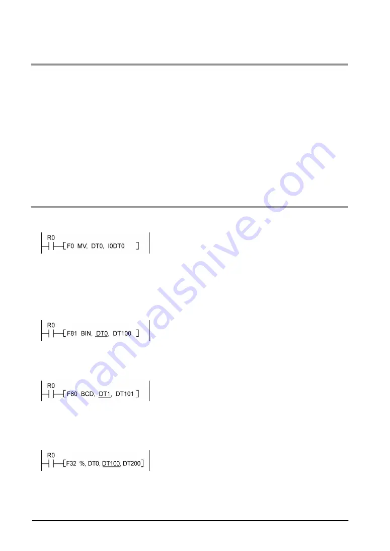
1. Check if an extraordinarily large value or negative value was stored in the index register.
<Example> When a data register is modified using an index register
In this case, index register modifies the address of data register DT0. However, it may exceed the
addressable range of the data register depending on the data in I0. If the value exceeds the range, an
operation error will occur. The same is true when the contents of I0 are a negative value.
2. Is there any data which cannot be converted using BCD
↔
BIN data conversion?
<Example> When BCD-to-BIN conversion is attempted
In this case, if DT0 contains a hexadecimal number with one of the digits A through F such as 12A4,
conversion will be impossible and an operation error will result.
<Example> When BIN-to-BCD conversion is attempted
In this case, if DT1 contains a negative value or a value greater than K9999, an operation error will occur.
3. Check if the devisor of a division instruction is “0”.
<Example>
In this case, if the content of DT100 is "0", an operation error will occur.
Summary of Contents for FP0R Series
Page 1: ......
Page 6: ...iv ...
Page 14: ...xii ...
Page 15: ...Chapter 1 Functions and Restrictions of the Unit ...
Page 24: ...1 10 ...
Page 25: ...Chapter 2 Specifications and Functions of Control Unit ...
Page 38: ...2 14 ...
Page 39: ...Chapter 3 Expansion ...
Page 45: ...3 7 3 4 Terminal layout diagram Model No Terminal layout diagrams E8RS E8RM E16RS E16RM E8YRS ...
Page 48: ...3 10 ...
Page 49: ...Chapter 4 I O Allocation ...
Page 53: ...Chapter 5 Installation and Wiring ...
Page 73: ...Chapter 6 Preparation of USB Port ...
Page 77: ...6 5 5 Click Finish on the following screen to be displayed ...
Page 79: ...6 7 4 Double click on FP0R 5 Click Update Driver ...
Page 84: ...6 12 ...
Page 85: ...Chapter 7 Communication ...
Page 139: ...7 55 Sample program For Type II Use a program as below to directly specify a MODBUS address ...
Page 141: ...Chapter 8 High speed Counter Pulse Output and PWM Output Functions ...
Page 142: ...8 2 ...
Page 199: ...Chapter 9 Security Functions ...
Page 211: ...Chapter 10 Other Functions ...
Page 217: ...Chapter 11 Self Diagnostic and Troubleshooting ...
Page 227: ...Chapter 12 Precautions During Programming ...
Page 242: ...12 16 ...
Page 243: ...Chapter 13 Specifications ...
Page 254: ...13 12 ...
Page 255: ...Chapter 14 Dimensions and Others ...
Page 262: ...14 8 ...
Page 263: ...Chapter 15 Appendix ...
Page 344: ...15 82 15 7 ASCII Codes ...
Page 346: ......
Page 347: ......
Page 348: ......


