background image

Rev. 1.10

158

October 23, 2020

Rev. 1.10 

159

October 23, 2020

BC66F5652

2.4GHz RF Transceiver A/D Flash MCU

BC66F5652

2.4GHz RF Transceiver A/D Flash MCU

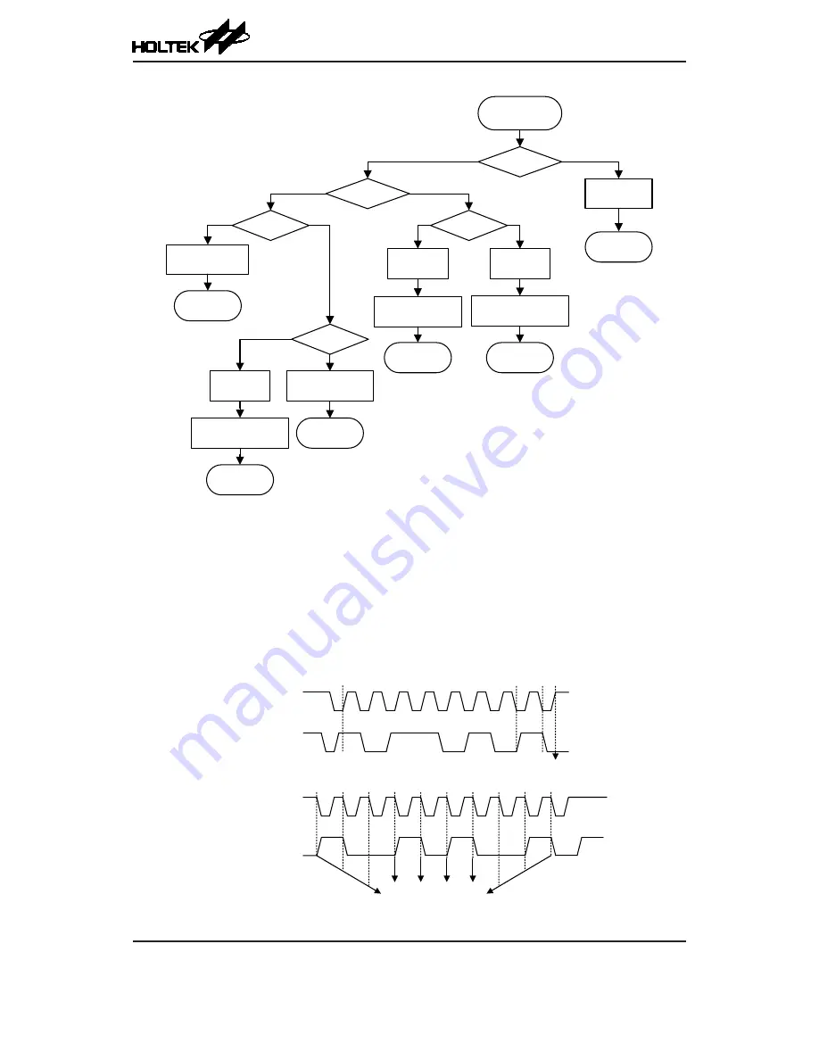
Start

SIMTOF=1?

SET SIMTOEN

CLR SIMTOF

RETI

HAAS=1?

HTX=1?

SRW=1?

Read from SIMD to 

release SCL Line

RETI

RXAK=1?

Write data to SIMD to 

release SCL Line

CLR HTX

CLR TXAK

Dummy read from SIMD 

to release SCL Line

RETI

RETI

SET HTX

Write data to SIMD to 

release SCL Line

RETI

CLR HTX

CLR TXAK

Dummy read from SIMD 

to release SCL Line

RETI

Yes

No

No

Yes

Yes

No

Yes

No

No

Yes

I

2

C Bus ISR Flow Chart

I

2

C Time-out Control

In order to reduce the I

2

C lockup problem due to reception of erroneous clock sources, a time-out 

function is provided. If the clock source connected to the I

2

C bus is not received for a while, then the 

I

2

C circuitry and registers will be reset after a certain time-out period. The time-out counter starts 

to count on an I

2

C bus “START” & “address match”

 condition, and is cleared by an SCL falling 

edge. Before the next SCL falling edge arrives, if the time elapsed is greater than the time-out period 

specified by the SIMTOC register, then a time-out condition will occur. The time-out function will 

stop when an I

2

C “STOP” condition occurs.

Start

SCL

SDA

SCL

SDA

1

0

ACK

Slave Address

SRW

Stop

1

1

0

1

0

1

0

1

0

0

1

0

1

0

0

I

2

C time-out 

counter start

I

2

C time-out counter reset 

on SCL negative transition

I

2

C Time-out

Summary of Contents for BC66F5652

Page 1: ...2 4GHz RF Transceiver A D Flash MCU BC66F5652 Revision V1 10 Date October 23 2020 ...

Page 2: ...ic Oscillator HXT 18 Low Speed Internal Oscillator Characteristics LIRC 18 External Low Speed Crystal Oscillator Characteristics LXT 18 Operating Frequency Characteristic Curves 18 System Start Up Time Characteristics 19 Input Output Characteristics 20 Memory Characteristics 20 A D Converter Electrical Characteristics 21 LVD LVR Electrical Characteristics 22 Reference Voltage Electrical Characteri...

Page 3: ...gister PCL 51 Look up Table Registers TBLP TBHP TBLH 51 Status Register STATUS 51 EEPROM Data Memory 53 EEPROM Data Memory Structure 53 EEPROM Registers 53 Read Operation from the EEPROM 55 Page Erase Operation to the EEPROM 55 Write Operation to the EEPROM 56 Oscillators 61 Oscillator Overview 61 System Clock Configurations 61 External Crystal Ceramic Oscillator HXT 62 Internal High Speed Interna...

Page 4: ...t Type TM CTM 94 Compact Type TM Operation 94 Compact Type TM Register Description 95 Compact Type TM Operating Modes 98 Standard Type TM STM 104 Standard Type TM Operation 104 Standard Type TM Register Description 104 Standard Type TM Operation Modes 108 Periodic Type TM PTM 118 Periodic Type TM Operation 118 Periodic Type TM Register Description 118 Periodic Type TM Operation Modes 122 Analog to...

Page 5: ...aging Receiver Errors 171 UART Interrupt Structure 172 UART Power Down and Wake up 173 SCOM SSEG Function for LCD 174 LCD Operation 174 LCD Control Registers 175 Low Voltage Detector LVD 178 LVD Register 178 LVD Operation 178 Interrupts 179 Interrupt Registers 179 Interrupt Operation 184 External Interrupt 185 Comparator Interrupt 186 Multi function Interrupts 186 A D Converter Interrupt 186 Time ...

Page 6: ...on 218 Instruction Timing 218 Moving and Transferring Data 218 Arithmetic Operations 218 Logical and Rotate Operation 219 Branches and Control Transfer 219 Bit Operations 219 Table Read Operations 219 Other Operations 219 Instruction Set Summary 220 Table Conventions 220 Extended Instruction Set 222 Instruction Definition 224 Extended Instruction Definition 233 Package Information 240 SAW Type 46 ...

Page 7: ...pulation instruction Peripheral Features Flash Program Memory 8K 16 RAM Data Memory 512 8 True EEPROM Memory 128 8 Watchdog Timer function In Application Programming IAP 22 bidirectional I O lines Two external interrupt lines shared with I O pins Programmable I O port source current for LED applications Multiple Timer Modules for time measure input capture compare match output PWM output function ...

Page 8: ...ata Memory as well as an area of true EEPROM memory for storage of non volatile data such as serial numbers calibration data etc Analog features include a multi channel 12 bit A D converter and a comparator function Multiple and extremely flexible Timer Modules provide timing pulse generation and PWM output functions Communication with the outside world is catered for by including fully integrated...

Page 9: ... LXT Pin Shared With Port B C XT1 XT2 OSC1 OSC2 HT8 MCU Core Clock System Timers Digital Peripherals UART I O MUX Analog Peripherals 12 bit ADC AVDD AVDD 2 AVDD 4 VR VR 2 VR 4 PGA AVDD Analog to Digital Converter 1 Comparator CMP VBGREF VREFI Pin Shared With Port A VREF Pin Shared With Port A AN0 AN11 Pin Shared With Port A B D C C CX Pin Shared With Port B Pin Shared With Port A IAP Reset Circuit...

Page 10: ...10 PD3 CTP SSEG25 AN9 BC66F5652 BC66V5652 46 QFN A 1 2 3 4 5 6 7 8 9 10111213141516171819 202122 34 35 36 37 38 39 23 24 25 26 27 28 29 30 31 32 33 40 41 42 43 44 45 46 Note 1 If the pin shared pin functions have multiple outputs simultaneously the desired pin shared function is determined by the corresponding software control bits 2 The OCDSDA and OCDSCK pins are supplied as dedicated OCDS pins a...

Page 11: ...A ST CMOS ICP Data Address pin OCDSDA ST CMOS OCDS Data Address pin for EV chip only PA1 INT0 SDO SCOM1 SSEG1 IRQ PA1 PAS0 PAWU PAPU ST CMOS General purpose I O Register enabled pull high and wake up INT0 PAS0 INTEG INTC0 IFS ST External Interrupt 0 SDO PAS0 CMOS SPI serial data output SCOM1 PAS0 SCOM Software controlled LCD common output SSEG1 PAS0 SSEG Software controlled LCD segment output IRQ ...

Page 12: ...1 SSEG Software controlled LCD segment output AN5 PAS1 AN A D Converter analog input channel 5 VREF PAS1 AN A D Converter reference voltage input PA7 PTP PTPI SCOM7 SSEG7 AN6 PA7 PAS1 PAWU PAPU ST CMOS General purpose I O Register enabled pull high and wake up PTP PAS1 CMOS PTM output PTPI PAS1 ST PTM capture input SCOM7 PAS1 SCOM Software controlled LCD common output SSEG7 PAS1 SSEG Software cont...

Page 13: ...rter analog input channel 8 PB5 SCS C SCOM13 SSEG13 PB5 PBS1 PBPU ST CMOS General purpose I O Register enabled pull high SCS PBS1 IFS ST CMOS SPI slave select pin C PBS1 AN Comparator negative input SCOM13 PBS1 SCOM Software controlled LCD common output SSEG13 PBS1 SSEG Software controlled LCD segment output PB6 SCK SCL C SSEG14 SCOM14 PB6 PBS1 PBPU ST CMOS General purpose I O Register enabled pul...

Page 14: ...erter analog input channel 10 PD3 CTP SSEG25 AN9 PD3 PDS0 PDPU ST CMOS General purpose I O Register enabled pull high CTP PDS0 CMOS CTM output SSEG25 PDS0 SSEG Software controlled LCD segment output AN9 PDS0 AN A D Converter analog input channel 9 VDD AVDD VDD PWR Digital positive power supply AVDD PWR Analog positive power supply VSS AVSS VSS PWR Digital negative power supply AVSS PWR Analog nega...

Page 15: ...bled pull high and wake up CSN SPI chip select input low active Note The PC3 PC6 lines which are internally connected to the RF Transceiver lines SDIO GIO2 SCK and CSN respectively should be properly configured to control the RF transceiver operations Refer to the Input Output Ports and RF Transceiver chapters for more details Absolute Maximum Ratings Supply Voltage VSS 0 3V to 3 6V Input Voltage ...

Page 16: ...S fHIRC 16MHz 3 3 3 6 Operating Current Characteristics Ta 40 C 85 C Symbol Operation Mode Test Conditions Min Typ Max Unit VDD Conditions IDD SLOW Mode LIRC 3V fSYS 32kHz 10 20 μA SLOW Mode LXT 3V fSYS 32768Hz 10 20 μA FAST Mode HIRC 3V fSYS 8MHz 1 0 1 5 mA 2 7V fSYS 12MHz 1 2 2 2 mA 3V 1 50 2 75 3 3V fSYS 16MHz 3 2 4 8 mA FAST Mode HXT 3V fSYS 8MHz 1 0 1 5 mA 2 7V fSYS 12MHz 1 2 2 2 mA 3V 1 50 2...

Page 17: ...LT instruction execution thus stopping all instruction execution A C Characteristics For data in the following tables note that factors such as oscillator type operating voltage operating frequency and temperature etc can all exert an influence on the measured values High Speed Internal Oscillator HIRC During the program writing operation the writer will trim the HIRC oscillator at a user selected...

Page 18: ...z 3 3V 3 6V 16 MHz tSTART HXT Start Up Time 3V 40 C 85 C 25 ms Low Speed Internal Oscillator Characteristics LIRC Symbol Parameter Test Conditions Min Typ Max Unit VDD Temp fLIRC LIRC Frequency 3V 25 C 2 32 2 kHz 2 2V 3 6V 40 C 85 C 10 32 10 kHz tSTART LIRC Start up Time 100 μs External Low Speed Crystal Oscillator Characteristics LXT Symbol Parameter Test Conditions Min Typ Max Unit VDD Condition...

Page 19: ...re Reset System Reset Delay Time Reset Source from WDT Overflow Reset 14 16 18 tSRESET Minimum Software Reset Width to Reset 45 90 120 μs tACTV ROM Activation Time Wake up from Power Down Mode 32 64 μs Note 1 For the System Start up time values whether fSYS is on or off depends upon the mode type and the chosen fSYS system oscillator Details are provided in the System Operating Modes section 2 The...

Page 20: ...ck Input Pin Minimum Pulse Width 0 3 μs tINT External Interrupt Minimum Pulse Width 10 μs Note The RPH internal pull high resistance value is calculated by connecting to ground and enabling the input pin with a pull high resistor and then measuring the pin current at the specified supply voltage level Dividing the voltage by this measured current provides the RPH value Memory Characteristics Ta 40...

Page 21: ... 0 01B VREF VDD tADCK 0 5μs 4 4 LSB 3V SAINS 3 0 0000B SAVRS 1 0 01B VREF VDD tADCK 0 5μs SAINS 3 0 0000B SAVRS 1 0 01B VREF VDD tADCK 10μs IADC Additional Current for A D Converter Enable 3V No load tADCK 0 5μs 450 600 μA tADCK Clock Period 1 9V VDD 2 0V 2 0 10 0 μs 2 0V VDD 3 6V 0 5 10 0 tADS Sampling Time 4 tADCK tADC Conversion Time Includes A D Sample and Hold Time 16 tADCK tON2ST A D Convert...

Page 22: ...e For LVR enable VBGEN 0 LVD off on 18 μs For LVR disable VBGEN 0 LVD off on 150 tLVR Minimum Low Voltage Width to Reset 120 240 480 μs tLVD Minimum Low Voltage Width to Interrupt 60 120 240 μs ILVR Additional Current for LVR Enable 3V LVD disable 8 μA ILVD Additional Current for LVD Enable 3V LVR disable 8 μA Reference Voltage Electrical Characteristics Ta 40 C 85 C unless otherwise specified Sym...

Page 23: ...here the comparator positive input voltage is equal to VDD 1 2 and remains constant 2 Measured with comparator one input pin at VCM VDD 1 2 while the other pin input transition from VSS to VCM 100mV or from VDD to VCM 100mV 3 Load Condition CLOAD 50pF Load Condition Pin CLOAD VSS Software Controlled LCD Driver Electrical Characteristics Ta 40 C 85 C Symbol Parameter Test Conditions Min Typ Max Uni...

Page 24: ...n 7 mA IRX or ITX RX or TX Mode Current RX mode 250Kbps 17 mA RX mode 500Kbps 17 mA TX mode 0dBm POUT 17 mA TX mode 5dBm POUT 25 mA A C Characteristics Ta 25 C VDD 3 3V fXTAL 16MHz GFSK modulation with matching circuit and low high pass filter RF output is powered by VDD 3 3V unless otherwise specified Symbol Parameter Test Conditions Min Typ Max Unit RF Characteristics fRF RF Frequency Band 2402 ...

Page 25: ...ode ready TBD μs Crystal Oscillator fXTAL X tal Frequency 16 MHz ESR X tal Equivalent Series Resistance 100 Ω CLOAD X tal Capacitor Load 12 16 pF TOL X tal Tolerance 20 20 ppm tSU X tal Startup Time 49US with a 12pF CLOAD 1 ms 3225 SMD with a 12pF CLOAD 3 ms Power on Reset Characteristics Ta 40 C 85 C Symbol Parameter Test Conditions Min Typ Max Unit VDD Conditions VPOR VDD Start Voltage to Ensure...

Page 26: ...cost high volume production for controller applications Clocking and Pipelining The main system clock derived from either an HXT LXT HIRC or LIRC oscillator is subdivided into four internally generated non overlapping clocks T1 T4 The Program Counter is incremented at the beginning of the T1 clock during which time a new instruction is fetched The remaining T2 T4 clocks carry out the decoding and ...

Page 27: ... short program jump can be executed directly However as only this low byte is available for manipulation the jumps are limited to the present page of memory that is 256 locations When such program jumps are executed it should also be noted that a dummy cycle will be inserted Manipulating the PCL register may cause program branching so an extra cycle is needed to pre fetch Stack This is a special p...

Page 28: ...tions after which the result will be placed in the specified register As these ALU calculation or operations may result in carry borrow or other status changes the status register will be correspondingly updated to reflect these changes The ALU supports the following functions Arithmetic operations ADD ADDM ADC ADCM SUB SUBM SBC SBCM DAA LADD LADDM LADC LADCM LSUB LSUBM LSBC LSBCM LDAA Logic opera...

Page 29: ...ice reset for program initialisation After a device reset is initiated the program will jump to this location and begin execution Look up Table Any location within the Program Memory can be defined as a look up table where programmers can store fixed data To use the look up table the table pointer must first be configured by placing the address of the look up data to be retrieved in the table poin...

Page 30: ... be restored care should be taken to ensure its protection if both the main routine and Interrupt Service Routine use table read instructions If using the table read instructions the Interrupt Service Routines may change the value of the TBLH and subsequently cause errors if used again by the main routine As a rule it is recommended that simultaneous use of the table read instructions should be av...

Page 31: ...d serially in circuit using this 4 wire interface Data is downloaded and uploaded serially on a single pin with an additional line for the clock Two additional lines are required for the power supply The technical details regarding the in circuit programming of the device are beyond the scope of this document and will be supplied in supplementary literature During the programming process the user ...

Page 32: ...tion the IAP interface can also be any type of communication protocol such as UART using I O pins Regarding the internal firmware the user can select versions provided by Holtek or create their own The following section illustrates the procedures regarding how to implement the IAP firmware Flash Memory Read Write Size The Flash memory Erase and Write operations are carried out in a page format whi...

Page 33: ... setting the CLWB bit high before the write buffer is used for the first time or when the data in the write buffer is updated The write buffer size is 32 words corresponding to a page The write buffer address is mapped to a specific flash memory page specified by the memory address bits FA12 FA5 The data written into the FD0L and FD0H registers will be loaded into the write buffer When data is wri...

Page 34: ...RH FA12 FA11 FA10 FA9 FA8 FD0L D7 D6 D5 D4 D3 D2 D1 D0 FD0H D15 D14 D13 D12 D11 D10 D9 D8 FD1L D7 D6 D5 D4 D3 D2 D1 D0 FD1H D15 D14 D13 D12 D11 D10 D9 D8 FD2L D7 D6 D5 D4 D3 D2 D1 D0 FD2H D15 D14 D13 D12 D11 D10 D9 D8 FD3L D7 D6 D5 D4 D3 D2 D1 D0 FD3H D15 D14 D13 D12 D11 D10 D9 D8 IAP Register List FARL Register Bit 7 6 5 4 3 2 1 0 Name FA7 FA6 FA5 FA4 FA3 FA2 FA1 FA0 R W R W R W R W R W R W R W R...

Page 35: ...D0 R W R W R W R W R W R W R W R W R W POR 0 0 0 0 0 0 0 0 Bit 7 0 D7 D0 The second Flash Memory data bit 7 bit 0 FD1H Register Bit 7 6 5 4 3 2 1 0 Name D15 D14 D13 D12 D11 D10 D9 D8 R W R W R W R W R W R W R W R W R W POR 0 0 0 0 0 0 0 0 Bit 7 0 D15 D8 The second Flash Memory data bit 15 bit 8 FD2L Register Bit 7 6 5 4 3 2 1 0 Name D7 D6 D5 D4 D3 D2 D1 D0 R W R W R W R W R W R W R W R W R W POR 0...

Page 36: ...served 110 Flash Memory Erase Write function Enable Mode 111 Reserved These bits are used to select the Flash Memory operation modes Note that the Flash memory Erase Write function Enable Mode should first be successfully enabled before the Erase or Write Flash memory operation is executed Bit 3 FWPEN Flash Memory Erase Write function enable procedure trigger 0 Erase Write function enable procedur...

Page 37: ...t 7 2 Unimplemented read as 0 Bit 1 FWERTS Erase time and Write time selection 0 Erase time is 3 2ms tFER Write time is 2 2ms tFWR 1 Erase time is 3 7ms tFER Write time is 3 0ms tFWR Bit 0 CLWB Flash Memory Write buffer clear control 0 Do not initiate a Write Buffer Clear process or indicating that a Write Buffer Clear process has completed 1 Initiate a Write Buffer Clear process This bit is set b...

Page 38: ... specific page Refer to the Flash Memory Write Procedure for details 5 Execute the TABRD instruction to read the flash memory contents and check if the written data is correct or not If the data read from the flash memory is different from the written data it means that the page write operation has failed The CLWB bit should be set high to clear the write buffer and then write the data into the sp...

Page 39: ...o the Flash data registers FD1L FD3L and FD1H FD3H as soon as possible after the FWPEN bit is set high The enable Flash memory erase write function data pattern is 00H 0DH C3H 04H 09H and 40H corresponding to the FD1L FD3L and FD1H FD3H registers respectively 4 Once the timer has timed out the FWPEN bit will automatically be cleared to zero by hardware regardless of the input data pattern 5 If the...

Page 40: ...tern to Flash Data register FD1L 00h FD1H 04h FD2L 0Dh FD2H 09h FD3L C3h FD3H 40h Is pattern correct CFWEN 0 Flash Memory Erase Write Function Disabled No CFWEN 1 Flash Memory Erase Write Function Enabled Yes END Is timer Time out FWPEN 0 No Yes Flash Memory Erase Write Function Enable Procedure Flash Memory Erase Write Function Enable Procedure ...

Page 41: ...y the address will not be further incremented but will stop at the last address of the page 1 Activate the Flash Memory Erase Write function enable procedure Check the CFWEN bit value and then execute the erase write operations if the CFWEN bit is set high Refer to the Flash Memory Erase Write function enable procedure for more details 2 Set the FMOD field to 001 to select the erase operation and ...

Page 42: ...t No Yes Blank Check with Table Read instruction Blank Check Page Data 0000h No Set CLWB bit Specify Flash Memory Address FARH xxH FARL xxH Yes Page Erase FMOD 2 0 001 Set CLWB Bit Set Erase Page Address FARH xxH FARL xxH Write dummy data into FD0H Tag Address Tag address Finish Yes No Flash Memory Consecutive Write Procedure Note 1 When the erase or write operation is successfully activated all C...

Page 43: ...fully completed Go to step 2 if the erase operation is not successful Go to step 4 if the erase operation is successful 4 Set the FMOD field to 000 to select the write operation 5 Setup the desired address ADDR1 in the FARH and FARL registers Write the desired data word DATA1 first into the FD0L register and then into the FD0H register 6 Set the FWT bit high to transfer the data word from the writ...

Page 44: ...ss FARH xxH FARL xxH Write another word Yes Yes Write Flash Memory Flash Memory Erase Write Function Enable Procedure FWT 1 Page Erase FMOD 2 0 001 Set CLWB Bit Set Erase Page Address FARH xxH FARL xxH Write dummy data into FD0H Tag Address Tag address Finish Yes No Flash Memory Non Consecutive Write Procedure Note 1 When the erase or write operation is successfully activated all CPU operations wi...

Page 45: ...he flash memory is correct 5 The system frequency should be setup to the maximum application frequency when data write and data check operations are executed using the IAP function Flash Memory Read Procedure To activate the Flash Memory Read procedure the FMOD field should be set to 011 to select the flash memory read mode and the FRDEN bit should be set high to enable the read function The desir...

Page 46: ...ccessible under program control Switching between the different Data Memory sectors is achieved by properly setting the Memory Pointers to correct value Structure The Data Memory is subdivided into several sectors all of which are implemented in 8 bit wide RAM Each of the Data Memory Sector is categorized into two types the special Purpose Data Memory and the General Purpose Data Memory The addres...

Page 47: ...s has 11 valid bits the high byte indicates a sector and the low byte indicates a specific address within the sector General Purpose Data Memory All microcontroller programs require an area of read write memory where temporary data can be stored and retrieved for use later It is this area of RAM memory that is known as General Purpose Data Memory This area of Data Memory is fully accessible by the...

Page 48: ...UCR1 USR PDPU PDC PD IFS SLEDC1 MFI2 MFI1 MFI0 TB1C VBGRC SIMTOC SIMC2 SIMA SIMD SIMC1 SIMC0 LXTC PCPU PCC PC EEC 40H 41H 42H 43H 44H 45H 46H 47H 48H 49H 4AH 4BH 4CH 4DH 4EH 4FH 50H 51H 52H 59H 58H 5BH 5AH 5DH 5CH 5FH 53H 54H 55H 56H 57H 5EH 60H 61H 62H 69H 68H 6BH 6AH 6DH 6CH 6FH 6EH 63H 64H 65H 66H 67H 70H 71H 72H 78H 7CH 73H 74H 75H 76H 77H 7BH 79H 7AH 7DH 7FH 7EH Sector 1 Sector 0 Sector 1 Sec...

Page 49: ... to the registers will result in no operation Memory Pointers MP0 MP1L MP1H MP2L MP2H Five Memory Pointers known as MP0 MP1L MP1H MP2L MP2H are provided These Memory Pointers are physically implemented in the Data Memory and can be manipulated in the same way as normal registers providing a convenient way with which to address and track data When any operation to the relevant Indirect Addressing R...

Page 50: ...c lsub a m 1 compare m and m 1 data snz c m m 1 jmp continue no lmov a m yes exchange m and m 1 data mov temp a lmov a m 1 lmov m a mov a temp lmov m 1 a continue Note Here m is a data memory address located in any data memory sectors For example m 1F0H it indicates address 0F0H in Sector 1 Accumulator ACC The Accumulator is central to the operation of any microcontroller and is closely related wi...

Page 51: ...ions like most other registers Any data written into the status register will not change the TO or PDF flag In addition operations related to the status register may give different results due to the different instruction operations The TO flag can be affected only by a system power up a WDT time out or by executing the CLR WDT or HALT instruction The PDF flag is affected only by executing the HAL...

Page 52: ...lag 0 After power up or executing the CLR WDT or HALT instruction 1 A watchdog time out occurred Bit 4 PDF Power down flag 0 After power up or executing the CLR WDT instruction 1 By executing the HALT instruction Bit 3 OV Overflow flag 0 No overflow 1 An operation results in a carry into the highest order bit but not a carry out of the highest order bit or vice versa Bit 2 Z Zero flag 0 The result...

Page 53: ...ctor 0 and a single control register in Sector 1 EEPROM Registers Three registers control the overall operation of the internal EEPROM Data Memory These are the address register EEA the data register EED and a single control register EEC As both the EEA and EED registers are located in Sector 0 they can be directly accessed in the same way as any other Special Function Register The EEC register ho...

Page 54: ...hen the bit is set high by the application program the Page write erase or read function will be selected Otherwise the byte write or read function will be selected The EEPROM page buffer size is 16 bytes Bit 3 WREN Data EEPROM Write Enable 0 Disable 1 Enable This is the Data EEPROM Write Enable Bit which must be set high before Data EEPROM write operations are carried out Clearing this bit to zer...

Page 55: ... address of the desired EEPROM page must first be placed in the EEA register as well as the read enable bit RDEN in the EEC register should be set high to enable the read function Then setting the RD bit high will initiate the EEPROM page read operation Note that setting the RD bit high only will not initiate a read operation if the RDEN bit is not set high When the current byte read cycle termina...

Page 56: ...00H after a page erase operation Write Operation to the EEPROM Writing data to the EEPROM can be implemented by two modes for this device byte write mode or page write mode which is controlled by the EEPROM operation mode selection bit MODE in the EEC register Byte Write Mode The EEPROM byte write operation can be executed when the mode selection bit MODE is cleared to zero For byte write operatio...

Page 57: ...mer whose operation is asynchronous to microcontroller system clock a certain time will elapse before the data will have been written into the EEPROM Detecting when the write cycle has finished can be implemented either by polling the WR bit in the EEC register or by using the EEPROM interrupt When the write cycle terminates the WR bit will be automatically cleared to zero by the microcontroller i...

Page 58: ... operation is totally complete Otherwise the EEPROM read or write operation will fail Programming Examples Reading a Data Byte from the EEPROM polling method MOV A 040H setup memory pointer low byte MP1L MOV MP1L A MP1 points to EEC register MOV A 01H setup memory pointer high byte MP1H MOV MP1H A CLR IAR1 4 clear MODE bit select byte operation mode MOV A EEPROM_ADRES user defined address MOV EEA ...

Page 59: ...T The data length can be up to 16 bytes End WRITE_BUF MOV A EEPROM_DATA user defined data erase mode don t care data value MOV EED A RET Erase_START CLR EMI SET IAR1 6 set EREN bit enable erase operations SET IAR1 5 start Erase Cycle set ER bit SET EMI BACK SZ IAR1 5 check for erase cycle end JMP BACK CLR MP1H Writing a Data Byte to the EEPROM polling method MOV A 040H setup Memory Pointer MP1L MO...

Page 60: ... select page operation mode MOV A EEPROM_ADRES user defined address MOV EEA A The data length can be up to 16 bytes Start CALL WRITE_BUF CALL WRITE_BUF JMP WRITE_START The data length can be up to 16 bytes End WRITE_BUF MOV A EEPROM_DATA user defined data MOV EED A RET WRITE_START CLR EMI SET IAR1 3 set WREN bit enable write operations SET IAR1 2 start Write Cycle set WR bit executed immediately a...

Page 61: ...tant in power sensitive portable applications Type Name Frequency Pins External High Speed Crystal Oscillator HXT 400kHz 16MHz OSC1 OSC2 Internal High Speed RC Oscillator HIRC 8 12 16MHz External Low Speed Crystal Oscillator LXT 32 768kHz XT1 XT2 Internal Low Speed RC Oscillator LIRC 32kHz Oscillator Types System Clock Configurations There are four methods of generating the system clock two high s...

Page 62: ...wo small value capacitors C1 and C2 Using a ceramic resonator will usually require two small value capacitors C1 and C2 to be connected as shown for oscillation to occur The values of C1 and C2 should be selected in consultation with the crystal or resonator manufacturer s specification For oscillator stability and to minimise the effects of noise and crosstalk it is important to ensure that the c...

Page 63: ... crystal are necessary to provide oscillation For applications where precise frequencies are essential these components may be required to provide frequency compensation due to different crystal manufacturing tolerances After the LXT oscillator is enabled by setting the LXTEN bit to 1 there is a time delay associated with the LXT oscillator waiting for it to start up When the microcontroller enter...

Page 64: ...onsume as little power as possible conflicting requirements that are especially true in battery powered portable applications The fast clocks required for high performance will by their nature increase current consumption and of course vice versa lower speed clocks reduce current consumption As Holtek has provided the device with both high and low speed clock sources and the means to switch betwee...

Page 65: ...ent modes of operation for the microcontroller each one with its own special characteristics and which can be chosen according to the specific performance and power requirements of the application There are two modes allowing normal operation of the microcontroller the FAST Mode and SLOW Mode The remaining four modes the SLEEP IDLE0 IDLE1 and IDLE2 Mode are used when the microcontroller CPU is swi...

Page 66: ...opped too However the fLIRC clock can continue to operate if the WDT function is enabled by the WDTC register IDLE0 Mode The IDLE0 Mode is entered when a HALT instruction is executed and when the FHIDEN bit in the SCC register is low and the FSIDEN bit in the SCC register is high In the IDLE0 Mode the CPU will be switched off but the low speed oscillator will be turned on to drive some peripheral ...

Page 67: ...e This bit is used to control whether the high speed oscillator is activated or stopped when the CPU is switched off by executing an HALT instruction Bit 0 FSIDEN Low Frequency oscillator control when CPU is switched off 0 Disable 1 Enable This bit is used to control whether the low speed oscillator is activated or stopped when the CPU is switched off by executing an HALT instruction HIRCC Registe...

Page 68: ...oscillator it is invalid to change the value of this bit Otherwise this bit value can be changed with no operation on the HXT function Bit 1 HXTF HXT oscillator stable flag 0 HXT unstable 1 HXT stable This bit is used to indicate whether the HXT oscillator is stable or not When the HXTEN bit is set high to enable the HXT oscillator the HXTF bit will first be cleared to zero and then set high after...

Page 69: ...ST fSYS fH fH 64 fH on CPU run fSYS on fSUB on SLOW fSYS fSUB fSUB on CPU run fSYS on fH on off IDLE0 HALT instruction executed CPU stop FHIDEN 0 FSIDEN 1 fH off fSUB on IDLE1 HALT instruction executed CPU stop FHIDEN 1 FSIDEN 1 fH on fSUB on IDLE2 HALT instruction executed CPU stop FHIDEN 1 FSIDEN 0 fH on fSUB off SLEEP HALT instruction executed CPU stop FHIDEN 0 FSIDEN 0 fH off fSUB off FAST Mod...

Page 70: ...nd then the system clock will respectively be switched to fH fH 64 However if fH is not used in SLOW mode and thus switched off it will take some time to re oscillate and stabilise when switching to the FAST mode from the SLOW Mode This is monitored using the HXTF bit in the HXTC register or the HIRCF bit in the HIRCC register The time duration required for the high speed system oscillator stabili...

Page 71: ...t the HALT instruction but the fSUB clock will be on The Data Memory contents and registers will maintain their present condition The I O ports will maintain their present conditions In the status register the Power Down flag PDF will be set and WDT timeout flag TO will be cleared The WDT will be cleared and resume counting if the WDT function is enabled If the WDT function is disabled the WDT wil...

Page 72: ...um current is drawn or connected only to external circuits that do not draw current such as other CMOS inputs Also note that additional standby current will also be required if the LXT or LIRC oscillator has enabled via configuration option In the IDLE1 and IDLE2 Mode the system oscillator is on if the peripheral function clock source is derived from the high speed oscillator the additional standb...

Page 73: ...ator is not ready yet when the first instruction is executed There are peripheral functions such as TMs for which the fSYS is used If the system clock source is switched from fH to fSUB the clock source to the peripheral functions mentioned above will change accordingly Watchdog Timer The Watchdog Timer is provided to prevent program malfunctions or sequences from jumping to unknown locations due ...

Page 74: ...set when its timer overflows This means that in the application program and during normal operation the user has to strategically clear the Watchdog Timer before it overflows to prevent the Watchdog Timer from executing a reset This is done using the clear watchdog instruction If the program malfunctions for whatever reason jumps to an unknown location or enters an endless loop the clear instructi...

Page 75: ...arameters The most important reset condition is after power is first applied to the microcontroller In this case internal circuitry will ensure that the microcontroller after a short delay will be in a well defined state and ready to execute the first program instruction After this power on reset certain important internal registers will be set to defined states before the program commences One of...

Page 76: ...C0 R W R W R W R W R W R W R W R W R W POR 0 1 0 1 0 1 0 1 Bit 7 0 RSTC7 RSTC0 Reset function control 01010101 No operation 10101010 No operation Other values Reset MCU If these bits are changed due to adverse environmental conditions the microcontroller will be reset The reset operation will be activated after a delay time tSRESET and the RSTF bit in the RSTFC register will be set to 1 RSTFC Regi...

Page 77: ...VR value can be selected by the LVS bits in the LVRC register If the LVS7 LVS0 bits are changed to some different values by environmental noise the LVR will reset the device after a delay time tSRESET When this happens the LRF bit in the RSTFC register will be set high After power on the register will have the value of 01100110B Note that the LVR function will be automatically disabled when the de...

Page 78: ...ftware reset flag Refer to the Watchdog Timer Control Register section IAP Reset When a specific value of 55H is written into the FC1 register a reset signal will be generated to reset the whole device Refer to the In Application Programming section for more associated details Watchdog Time out Reset during Normal Operation The Watchdog time out Reset during normal operation is the same as the LVR...

Page 79: ...wing table describes how each type of reset affects each of the microcontroller internal registers Register Name Reset Power On LVR Reset WDT Time out Normal Operation WDT Time out IDLE SLEEP IAR0 0 0 0 0 0 0 0 0 0 0 0 0 0 0 0 0 0 0 0 0 0 0 0 0 u u u u u u u u MP0 0 0 0 0 0 0 0 0 0 0 0 0 0 0 0 0 0 0 0 0 0 0 0 0 u u u u u u u u IAR1 0 0 0 0 0 0 0 0 0 0 0 0 0 0 0 0 0 0 0 0 0 0 0 0 u u u u u u u u MP...

Page 80: ...0 0 0 0 0 0 0 0 0 u u u u u CTMC1 0 0 0 0 0 0 0 0 0 0 0 0 0 0 0 0 0 0 0 0 0 0 0 0 u u u u u u u u CTMDL 0 0 0 0 0 0 0 0 0 0 0 0 0 0 0 0 0 0 0 0 0 0 0 0 u u u u u u u u CTMDH 0 0 0 0 0 0 0 0 0 0 0 0 0 0 0 0 0 0 0 0 0 0 0 0 u u u u u u u u CTMAL 0 0 0 0 0 0 0 0 0 0 0 0 0 0 0 0 0 0 0 0 0 0 0 0 u u u u u u u u CTMAH 0 0 0 0 0 0 0 0 0 0 0 0 0 0 0 0 0 0 0 0 0 0 0 0 u u u u u u u u CTMRP 0 0 0 0 0 0 0 0 ...

Page 81: ...0 0 0 0 0 0 0 0 0 0 0 0 0 0 0 0 u u u u u u u u BRG x x x x x x x x x x x x x x x x x x x x x x x x u u u u u u u u TXR_RXR x x x x x x x x x x x x x x x x x x x x x x x x u u u u u u u u LVPUC 0 0 0 u PAS0 0 0 0 0 0 0 0 0 0 0 0 0 0 0 0 0 0 0 0 0 0 0 0 0 u u u u u u u u PAS1 0 0 0 0 0 0 0 0 0 0 0 0 0 0 0 0 0 0 0 0 0 0 0 0 u u u u u u u u PBS0 0 0 0 0 0 0 0 0 0 0 0 0 0 0 0 0 0 0 0 0 0 0 0 0 u u u u...

Page 82: ...n these ports are non latching which means the inputs must be ready at the T2 rising edge of instruction MOV A m where m denotes the port address For output operation all the data is latched and remains unchanged until the output latch is rewritten Register Name Bit 7 6 5 4 3 2 1 0 PA PA7 PA6 PA5 PA4 PA3 PA2 PA1 PA0 PAC PAC7 PAC6 PAC5 PAC4 PAC3 PAC2 PAC1 PAC0 PAPU PAPU7 PAPU6 PAPU5 PAPU4 PAPU3 PAP...

Page 83: ...rresponding PCPU3 PCPU6 bits in the PCPU register should be properly configured after power on LVPUC Register Bit 7 6 5 4 3 2 1 0 Name LVPU R W R W POR 0 Bit 7 1 Unimplemented read as 0 Bit 0 LVPU Pull high resistor selection when low voltage power supply 0 All pin pull high resistors are 60kΩ 3V 1 All pin pull high resistors are 15kΩ 3V This bit is used to select the pull high resistor value for ...

Page 84: ...t pin PxC Register Bit 7 6 5 4 3 2 1 0 Name PxC7 PxC6 PxC5 PxC4 PxC3 PxC2 PxC1 PxC0 R W R W R W R W R W R W R W R W R W POR 1 1 1 1 1 1 1 1 PxCn I O Port x Pin type selection 0 Output 1 Input The PxCn bit is used to control the pin type selection Here the x can be A B C or D However the actual available bits for each I O Port may be different Note that the PC3 PC6 lines are not connected to the ex...

Page 85: ... 1 10 Source current Level 2 11 Source current Level 3 Max SLEDC1 Register Bit 7 6 5 4 3 2 1 0 Name SLEDC15 SLEDC14 D3 D2 SLEDC11 SLEDC10 R W R W R W R W R W R W R W POR 0 0 0 0 0 0 Bit 7 6 Unimplemented read as 0 Bit 5 4 SLEDC15 SLEDC14 PD3 PD0 Source Current Selection 00 Source current Level 0 Min 01 Source current Level 1 10 Source current Level 2 11 Source current Level 3 Max Bit 3 2 D3 D2 The...

Page 86: ...rol configuration with their corresponding general purpose I O functions when setting the relevant pin shared control bit fields To select these pin functions in addition to the necessary pin shared control and peripheral functional setup aforementioned they must also be setup as an input by setting the corresponding bit in the I O port control register To correctly deselect the pin shared functio...

Page 87: ...SSEG0 PAS1 Register Bit 7 6 5 4 3 2 1 0 Name PAS17 PAS16 PAS15 PAS14 PAS13 PAS12 PAS11 PAS10 R W R W R W R W R W R W R W R W R W POR 0 0 0 0 0 0 0 0 Bit 7 6 PAS17 PAS16 PA7 Pin Shared Function Selection 00 PA7 PTPI 01 PTP 10 SCOM7 SSEG7 11 AN6 Bit 5 4 PAS15 PAS14 PA6 Pin Shared Function Selection 00 PA6 CTCK 01 SCOM6 SSEG6 10 AN5 11 VREF Bit 3 2 PAS13 PAS12 PA5 Pin Shared Function Selection 00 PA5...

Page 88: ...SCL 10 C 11 SCOM14 SSEG14 Bit 3 2 PBS13 PBS12 PB5 Pin Shared function selection 00 PB5 01 SCS 10 C 11 SCOM13 SSEG13 Bit 1 0 PBS11 PBS10 PB4 Pin Shared function selection 00 PB4 01 CLO 10 SCOM12 SSEG12 11 AN8 PCS0 Register Bit 7 6 5 4 3 2 1 0 Name D7 D6 PCS05 PCS04 PCS03 PCS02 PCS01 PCS00 R W R W R W R W R W R W R W R W R W POR 0 0 0 0 0 0 0 0 Bit 7 6 D7 D6 These bits should be kept unchanged after...

Page 89: ...SSEG23 11 AN11 Bit 1 0 PCS01 PCS00 PD0 Pin Shared Function Selection 00 PD0 01 PD0 10 PTP 11 SSEG22 IFS Register Bit 7 6 5 4 3 2 1 0 Name INT1PS INT0PS SDI_SDAPS SCK_SCLPS SCSBPS RXPS R W R W R W R W R W R W R W POR 0 0 0 0 0 0 Bit 7 6 Unimplemented read as 0 Bit 5 INT1PS INT1 input source pin selection 0 PB1 1 PA2 Bit 4 INT0PS INT0 input source pin selection 0 PB0 1 PA1 Bit 3 SDI_SDAPS SDI SDA in...

Page 90: ... that all I O pins will default to an input state the level of which depends on the other connected circuitry and whether pull high selections have been chosen If the port control registers are then programmed to set some pins as outputs these output pins will have an initial high output value unless the associated port data registers are first programmed Selecting which pins are inputs and which ...

Page 91: ... main features and differences between the three types of TMs are summarised in the accompanying table TM Function CTM STM PTM Timer Counter Input Capture Compare Match Output PWM Output Single Pulse Output PWM Alignment Edge Edge Edge PWM Adjustment Period Duty Duty or Period Duty or Period Duty or Period TM Function Summary TM Operation The different types of TM offer a diverse range of function...

Page 92: ...nd PTM respectively For STM and PTM another input pin STPI or PTPI is the capture input whose active edge can be a rising edge a falling edge or both rising and falling edges and the active edge transition type is selected using the STIO1 STIO0 or PTIO1 PTIO0 bits in the STMC1 or PTMC1 register respectively There is another capture input PTCK for PTM capture input mode which can be used as the ext...

Page 93: ...8 bit buffer and its related low byte only takes place when a write or read operation to its corresponding high byte is executed As the CCRA and CCRP registers are implemented in the way shown in the following diagram and accessing these register pairs is carried out in a specific way as described above it is recommended to use the MOV instruction to access the CCRA and CCRP low byte registers nam...

Page 94: ...AF Interrupt CTMPF Interrupt CTPOL PxSn CCRA CTCCLR Note the CTM external pins are pin shared with other functions so before using the CTM function ensure that the pin shared function registers have been set properly to enable the CTM pin function The CTCK pin if used must also be set as an input by setting the corresponding bit in the port control register 16 bit Compact Type TM Block Diagram Com...

Page 95: ...ter operation When in a Pause condition the CTM will remain powered up and continue to consume power The counter will retain its residual value when this bit changes from low to high and resume counting from this value when the bit changes to a low value again Bit 6 4 CTCK2 CTCK0 CTM counter clock selection 000 fSYS 4 001 fSYS 010 fH 16 011 fH 64 100 fSUB 101 fSUB 110 CTCK rising edge clock 111 CT...

Page 96: ...t depends upon in which mode the CTM is running In the Compare Match Output Mode the CTIO1 and CTIO0 bits determine how the CTM output pin changes state when a compare match occurs from the Comparator A The CTM output pin can be set to switch high switch low or to toggle its present state when a compare match occurs from the Comparator A When the bits are both zero then no change will take place o...

Page 97: ...TM Comparator P match 1 CTM Comparator A match This bit is used to select the method which clears the counter Remember that the Compact TM contains two comparators Comparator A and Comparator P either of which can be selected to clear the internal counter With the CTCCLR bit set high the counter will be cleared when a compare match occurs from the Comparator A When the bit is low the counter will ...

Page 98: ... bits in the CTMC1 register Compare Match Output Mode To select this mode bits CTM1 and CTM0 in the CTMC1 register should be set to 00 respectively In this mode once the counter is enabled and running it can be cleared by three methods These are a counter overflow a compare match from Comparator A and a compare match from Comparator P When the CTCCLR bit is low there are two ways in which the coun...

Page 99: ...e Counter Value 0xFFFF CCRP CCRA CTON CTPAU CTPOL CCRP Int Flag CTMPF CCRA Int Flag CTMAF CTM O P Pin Time CCRP 0 CCRP 0 Counter overflow CCRP 0 Counter cleared by CCRP value Pause Resume Stop Counter Restart CTCCLR 0 CTM 1 0 00 Output pin set to initial Level Low if CTOC 0 Output Toggle with CTMAF flag Note CTIO 1 0 10 Active High Output select Here CTIO 1 0 11 Toggle Output select Output not aff...

Page 100: ...ut not affected by CTMAF flag Remains High until reset by CTON bit Output Pin Reset to Initial value Output controlled by other pin shared function Output Inverts when CTPOL is high CTMPF not generated No CTMAF flag generated on CCRA overflow Output does not change CTCCLR 1 CTM 1 0 00 CCRA Int Flag CTMAF CCRP Int Flag CTMPF Compare Match Output Mode CTCCLR 1 Note 1 With CTCCLR 1 a Comparator A mat...

Page 101: ...CRP registers are used to generate the PWM waveform one register is used to clear the internal counter and thus control the PWM waveform frequency while the other one is used to control the duty cycle Which register is used to control either frequency or duty cycle is determined using the CTDPX bit in the CTMC1 register The PWM waveform frequency and duty cycle can therefore be controlled by the v...

Page 102: ...WM Duty Cycle set by CCRA PWM resumes operation Output controlled by other pin shared function Output Inverts when CTPOL 1 PWM Period set by CCRP CTM O P Pin CTOC 0 CCRA Int Flag CTMAF CCRP Int Flag CTMPF CTDPX 0 CTM 1 0 10 PWM Output Mode CTDPX 0 Note 1 Here CTDPX 0 Counter cleared by CCRP 2 A counter clear sets the PWM Period 3 The internal PWM function continues even when CTIO 1 0 00 or 01 4 Th...

Page 103: ...w Counter Reset when CTON returns high PWM Duty Cycle set by CCRP PWM resumes operation Output controlled by other pin shared function Output Inverts when CTPOL 1 PWM Period set by CCRA CTM O P Pin CTOC 0 CTDPX 1 CTM 1 0 10 PWM Output Mode CTDPX 1 Note 1 Here CTDPX 1 Counter cleared by CCRA 2 A counter clear sets the PWM Period 3 The internal PWM function continues even when CTIO 1 0 00 or 01 4 Th...

Page 104: ...ser selectable internal or external clock source There are also two internal comparators with the names Comparator A and Comparator P These comparators will compare the value in the counter with CCRP and CCRA registers The CCRP comparator is 8 bit wide whose value is compared with the highest 8 bits in the counter while the CCRA is the sixteen bits and therefore compares all counter bits The only ...

Page 105: ...SYS 010 fH 16 011 fH 64 100 fSUB 101 fSUB 110 STCK rising edge clock 111 STCK falling edge clock These three bits are used to select the clock source for the STM The external pin clock source can be chosen to be active on the rising or falling edge The clock source fSYS is the system clock while fH and fSUB are other internal clocks the details of which can be found in the oscillator section Bit 3...

Page 106: ...eached The function that these bits select depends upon in which mode the STM is running In the Compare Match Output Mode the STIO1 and STIO0 bits determine how the STM output pin changes state when a compare match occurs from the Comparator A The TM output pin can be setup to switch high switch low or to toggle its present state when a compare match occurs from the Comparator A When the bits are ...

Page 107: ... CCRP duty CCRA period This bit determines which of the CCRA and CCRP registers are used for period and duty control of the PWM waveform Bit 0 STCCLR STM counter clear condition selection 0 Comparator P match 1 Comparator A match This bit is used to select the method which clears the counter Remember that the Standard TM contains two comparators Comparator A and Comparator P either of which can be...

Page 108: ...ternal counter As the CCRP bits are only compared with the highest eight counter bits the compare values exist in 256 clock cycle multiples Clearing all eight bits to zero is in effect allowing the counter to overflow at its maximum value Standard Type TM Operation Modes The Standard Type TM can operate in one of five operating modes Compare Match Output Mode PWM Output Mode Single Pulse Output Mo...

Page 109: ...r The STM output pin can be selected using the STIO1 and STIO0 bits to go high to go low or to toggle from its present condition when a compare match occurs from Comparator A The initial condition of the STM output pin which is setup after the STON bit changes from low to high is setup using the STOC bit Note that if the STIO1 and STIO0 bits are zero then no pin change will take place Counter Valu...

Page 110: ...igh Output select Here STIO 1 0 11 Toggle Output select Output not affected by STMAF flag Remains High until reset by STON bit Output Pin Reset to Initial value Output controlled by other pin shared function Output Inverts when STPOL is high STMPF not generated No STMAF flag generated on CCRA overflow Output does not change Compare Match Output Mode STCCLR 1 Note 1 With STCCLR 1 a Comparator A mat...

Page 111: ...RA and CCRP registers are used to generate the PWM waveform one register is used to clear the internal counter and thus control the PWM waveform frequency while the other one is used to control the duty cycle Which register is used to control either frequency or duty cycle is determined using the STDPX bit in the STMC1 register The PWM waveform frequency and duty cycle can therefore be controlled ...

Page 112: ...w Counter Reset when STON returns high STDPX 0 STM 1 0 10 PWM Duty Cycle set by CCRA PWM resumes operation Output controlled by other pin shared function Output Inverts when STPOL 1 PWM Period set by CCRP STM O P Pin STOC 0 PWM Output Mode STDPX 0 Note 1 Here STDPX 0 Counter cleared by CCRP 2 A counter clear sets the PWM Period 3 The internal PWM function continues even when STIO 1 0 00 or 01 4 Th...

Page 113: ...w Counter Reset when STON returns high STDPX 1 STM 1 0 10 PWM Duty Cycle set by CCRP PWM resumes operation Output controlled by other pin shared function Output Inverts when STPOL 1 PWM Period set by CCRA STM O P Pin STOC 0 PWM Output Mode STDPX 1 Note 1 Here STDPX 1 Counter cleared by CCRA 2 A counter clear sets the PWM Period 3 The internal PWM function continues even when STIO 1 0 00 or 01 4 Th...

Page 114: ... leading edge will be generated The STON bit should remain high when the pulse is in its active state The generated pulse trailing edge will be generated when the STON bit is cleared to zero which can be implemented using the application program or when a compare match occurs from Comparator A However a compare match from Comparator A will also automatically clear the STON bit and thus generate th...

Page 115: ...RA Output Inverts when STPOL 1 No CCRP Interrupts generated STM O P Pin STOC 0 STCK pin Software Trigger Cleared by CCRA match STCK pin Trigger Auto set by STCK pin Software Trigger Software Clear Software Trigger Software Trigger Single Pulse Output Mode Note 1 Counter stopped by CCRA 2 CCRP is not used 3 The pulse triggered by the STCK pin or by setting the STON bit high 4 A STCK pin active edge...

Page 116: ...in the present value in the counter will be latched into the CCRA registers and a STM interrupt generated Irrespective of what events occur on the STPI pin the counter will continue to free run until the STON bit changes from high to low When a CCRP compare match occurs the counter will reset back to zero in this way the CCRP value can be used to control the maximum counter value When a CCRP compa...

Page 117: ...op STIO 1 0 Value XX YY XX YY Active edge Active edge Active edge 00 Rising edge 01 Falling edge 10 Both edges 11 Disable Capture Capture Input Mode Note 1 STM 1 0 01 and active edge set by the STIO 1 0 bits 2 A STM Capture input pin active edge transfers the counter value to CCRA 3 STCCLR bit not used 4 No output function STOC and STPOL bits are not used 5 CCRP determines the counter value and th...

Page 118: ...10 bit wide and its core is a 10 bit count up counter which is driven by a user selectable internal or external clock source There are also two internal comparators with the names Comparator A and Comparator P These comparators will compare the value in the counter with CCRP and CCRA registers The CCRP and CCRA comparators are 10 bit wide whose value is compared with all counter bits The only way ...

Page 119: ... 011 fH 64 100 fSUB 101 fSUB 110 PTCK rising edge clock 111 PTCK falling edge clock These three bits are used to select the clock source for the PTM The external pin clock source can be chosen to be active on the rising or falling edge The clock source fSYS is the system clock while fH and fSUB are other internal clocks the details of which can be found in the oscillator section Bit 3 PTON PTM cou...

Page 120: ...ndition is reached The function that these bits select depends upon in which mode the PTM is running In the Compare Match Output Mode the PTIO1 and PTIO0 bits determine how the PTM output pin changes state when a compare match occurs from the Comparator A The PTM output pin can be setup to switch high switch low or to toggle its present state when a compare match occurs from the Comparator A When ...

Page 121: ...er Mode Bit 1 PTCAPTS PTM capture trigger source selection 0 From PTPI pin 1 From PTCK pin Bit 0 PTCCLR PTM counter clear condition selection 0 Comparator P match 1 Comparator A match This bit is used to select the method which clears the counter Remember that the Periodic TM contains two comparators Comparator A and Comparator P either of which can be selected to clear the internal counter With t...

Page 122: ... 0 PTM 10 bit CCRP bit 9 bit 8 Periodic Type TM Operation Modes The Periodic Type TM can operate in one of five operating modes Compare Match Output Mode PWM Output Mode Single Pulse Output Mode Capture Input Mode or Timer Counter Mode The operating mode is selected using the PTM1 and PTM0 bits in the PTMC1 register Compare Match Output Mode To select this mode bits PTM1 and PTM0 in the PTMC1 regi...

Page 123: ...the PTIO1 and PTIO0 bits in the PTMC1 register The PTM output pin can be selected using the PTIO1 and PTIO0 bits to go high to go low or to toggle from its present condition when a compare match occurs from Comparator A The initial condition of the PTM output pin which is setup after the PTON bit changes from low to high is setup using the PTOC bit Note that if the PTIO1 and PTIO0 bits are zero th...

Page 124: ...ere PTIO 1 0 11 Toggle Output select Output not affected by PTMAF flag Remains High until reset by PTON bit Output Pin Reset to Initial value Output controlled by other pin shared function Output Inverts when PTPOL is high PTMPF not generated No PTMAF flag generated on CCRA overflow Output does not change PTCCLR 1 PTM 1 0 00 Compare Match Output Mode PTCCLR 1 Note 1 With PTCCLR 1 a Comparator A ma...

Page 125: ...s As both the period and duty cycle of the PWM waveform can be controlled the choice of generated waveform is extremely flexible In the PWM Output Mode the PTCCLR bit has no effect as the PWM period Both of the CCRP and CCRA registers are used to generate the PWM waveform one register is used to clear the internal counter and thus control the PWM waveform frequency while the other one is used to c...

Page 126: ... bit low Counter Reset when PTON returns high PWM Duty Cycle set by CCRA PWM resumes operation Output controlled by other pin shared function Output Inverts When PTPOL 1 PWM Period set by CCRP PTM O P Pin PTOC 0 PTM 1 0 10 PWM Output Mode Note 1 The counter is cleared by CCRP 2 A counter clear sets the PWM Period 3 The internal PWM function continues running even when PTIO 1 0 00 or 01 4 The PTCCL...

Page 127: ...he pulse leading edge will be generated The PTON bit should remain high when the pulse is in its active state The generated pulse trailing edge will be generated when the PTON bit is cleared to zero which can be implemented using the application program or when a compare match occurs from Comparator A However a compare match from Comparator A will also automatically clear the PTON bit and thus gen...

Page 128: ...PTPOL 1 No CCRP Interrupts generated PTM O P Pin PTOC 0 PTCK pin Software Trigger Cleared by CCRA match PTCK pin Trigger Auto set by PTCK pin Software Trigger Software Clear Software Trigger Software Trigger PTM 1 0 10 PTIO 1 0 11 Single Pulse Output Mode Note 1 Counter stopped by CCRA 2 CCRP is not used 3 The pulse triggered by the PTCK pin or by setting the PTON bit high 4 A PTCK pin active edge...

Page 129: ...rated Irrespective of what events occur on the PTPI or PTCK pin the counter will continue to free run until the PTON bit changes from high to low When a CCRP compare match occurs the counter will reset back to zero in this way the CCRP value can be used to control the maximum counter value When a CCRP compare match occurs from Comparator P a PTM interrupt will also be generated Counting the number...

Page 130: ...r Stop PTIO 1 0 Value XX YY XX YY Active edge Active edge Active edge 00 Rising edge 01 Falling edge 10 Both edges 11 Disable Capture Capture Input Mode Note 1 PTM 1 0 01 and active edge set by the PTIO 1 0 bits 2 A PTM Capture input pin active edge transfers the counter value to CCRA 3 PTCCLR bit not used 4 No output function PTOC and PTPOL bits are not used 5 CCRP determines the counter value an...

Page 131: ... The external or internal analog signal to be converted is determined by the SAINS3 SAINS0 bits together with the SACS3 SACS0 bits Note that when the internal analog signal is to be converted using the SAINS bit field the external channel analog input will be automatically be switched off More detailed information about the A D converter input signal is described in the A D Converter Control Regis...

Page 132: ...sed the format in which the data is stored is controlled by the ADRFS bit in the SADC0 register as shown in the accompanying table D0 D11 are the A D conversion result data bits Any unused bits will be read as zero Note that the A D converter data register contents will keep unchanged if the A D converter is disabled ADRFS SADOH SADOL 7 6 5 4 3 2 1 0 7 6 5 4 3 2 1 0 0 D11 D10 D9 D8 D7 D6 D5 D4 D3 ...

Page 133: ...flag is used to indicate whether the A D conversion is in progress or not When the START bit is set from low to high and then to low again the ADBZ flag will be set high to indicate that the A D conversion is initiated The ADBZ flag will be cleared to zero after the A D conversion is complete Bit 5 ADCEN A D Converter function enable control 0 Disable 1 Enable This bit controls the A D converter i...

Page 134: ...value It will prevent the external channel input from being connected together with the internal analog signal Bit 3 Unimplemented read as 0 Bit 2 0 SACKS2 SACKS0 A D conversion clock source selection 000 fSYS 001 fSYS 2 010 fSYS 4 011 fSYS 8 100 fSYS 16 101 fSYS 32 110 fSYS 64 111 fSYS 128 SADC2 Register Bit 7 6 5 4 3 2 1 0 Name ADPGAEN PGAIS SAVRS1 SAVRS0 PGAGS1 PGAGS0 R W R W R W R W R W R W R ...

Page 135: ...onverter Reference Voltage The actual reference voltage supply to the A D Converter can be supplied from the internal A D converter power AVDD an external reference source supplied on pin VREF or an internal reference voltage VR determined by the SAVRS1 SAVRS0 bits in the SADC2 register The internal reference voltage is amplified through a programmable gain amplifier PGA which is controlled by the...

Page 136: ...ignal will be selected If the internal analog signal is selected to be converted the external channel signal input will automatically be switched off regardless of the SACS field value It will prevent the external channel input from being connected together with the internal analog signal SAINS 3 0 SACS 3 0 Input Signals Description 0000 0100 11xx 0000 1011 AN0 AN11 External channel analog input A...

Page 137: ...16MHz 62 5ns 125ns 250ns 500ns 1μs 2μs 4μs 8μs A D Conversion Clock Period Examples Controlling the power on off function of the A D conversion circuitry is implemented using the ADCEN bit in the SADC0 register This bit must be set high to power on the A D converter When the ADCEN bit is set high to power on the A D conversion internal circuitry a certain delay as indicated in the timing diagram m...

Page 138: ... be converted go to Step 5 Step 4 If the A D input signal comes from the external channel input selected by configuring the SAINS bit field the corresponding pin should first be configured as an A D input function by configuring the relevant pin function control bits The desired external channel input should be selected by configuring the SACS field After this step go to Step 6 Step 5 If the A D i...

Page 139: ...converter input lines are used as normal I Os then care must be taken as if the input voltage is not at a valid logic level then this may lead to some increase in power consumption A D Conversion Function As the device contains a 12 bit A D converter its full scale converted digitised value is equal to FFFH Since the full scale analog input value is equal to the actual A D converter reference volt...

Page 140: ...conversion polling_EOC sz ADBZ poll the SADC0 register ADBZ bit to detect end of A D conversion jmp polling_EOC continue polling mov a SADOL read low byte conversion result value mov SADOL_buffer a save result to user defined register mov a SADOH read high byte conversion result value mov SADOH_buffer a save result to user defined register jmp start_conversion start next A D conversion Example usi...

Page 141: ...ny pull high resistors connected to the shared comparator input pins will be automatically disconnected when the corresponding comparator functional pins are selected As the comparator inputs approach their switching level some spurious output signals may be generated on the comparator output due to the slow rising or falling nature of the input signals This can be minimised by the hysteresis func...

Page 142: ... and by the condition of the CMPPOL bit Bit 3 1 Unimplemented read as 0 Bit 0 CMPHYEN Comparator hysteresis voltage control 0 Comparator hysteresis disable 1 Comparator hysteresis enable Refer to Comparator Characteristics section Comparator Interrupt The comparator possesses its own interrupt function When the comparator output bit changes state its relevant interrupt flag will be set and if the ...

Page 143: ...nal hardware devices The communication is full duplex and operates as a slave master type where the device can be either master or slave Although the SPI interface specification can control multiple slave devices from a single master the device provides only one SCS pin If the master needs to control multiple slave devices from a single master the master can use I O pin to select the slave devices...

Page 144: ...face These are the SIMD data register and two registers SIMC0 and SIMC2 The SIMC1 register is only used by the I2 C interface Register Name Bit 7 6 5 4 3 2 1 0 SIMC0 SIM2 SIM1 SIM0 SIMDEB1 SIMDEB0 SIMEN SIMICF SIMC2 D7 D6 CKPOLB CKEG MLS CSEN WCOL TRF SIMD D7 D6 D5 D4 D3 D2 D1 D0 SPI Register List SPI Data Register The SIMD register is used to store the data being transmitted and received The same...

Page 145: ... C register section Bit 1 SIMEN SIM Enable Control 0 Disable 1 Enable The bit is the overall on off control for the SIM interface When the SIMEN bit is cleared to zero to disable the SIM interface the SDI SDO SCK and SCS or SDA and SCL lines will lose their SPI or I2 C function and the SIM operating current will be reduced to a minimum value When the bit is high the SIM interface is enabled If the...

Page 146: ...be generated The CKPOLB bit determines the base condition of the clock line if the bit is high then the SCK line will be low when the clock is inactive When the CKPOLB bit is low then the SCK line will be high when the clock is inactive The CKEG bit determines active clock edge type which depends upon the condition of CKPOLB bit Bit 3 MLS SPI data shift order 0 LSB first 1 MSB first This is the da...

Page 147: ...be transferred should be well prepared at the appropriate moment relative to the SCK signal depending upon the configurations of the CKPOLB bit and CKEG bit The accompanying timing diagram shows the relationship between the slave data and SCK signal for various configurations of the CKPOLB and CKEG bits The SPI will continue to function in certain IDLE Modes if the clock source used by the SPI int...

Page 148: ...loating if SCS 1 Note For SPI slave mode if SIMEN 1 and CSEN 0 SPI is always enabled and ignores the SCS level SPI Slave Mode Timing CKEG 1 Clear WCOL Write Data into SIMD WCOL 1 Transmission completed TRF 1 Read Data from SIMD Clear TRF END Transfer finished A SPI Transfer Master or Slave SIMEN 1 Configure CKPOLB CKEG CSEN and MLS A SIM 2 0 000 001 010 011 or 100 SIM 2 0 101 Master Slave Y Y N N ...

Page 149: ...on bit CKPOLB in the SIMC2 register If in Slave Mode the SCK line will be in a floating condition If the SIMEN bit is low then the bus will be disabled and SCS SDI SDO and SCK will all become I O pins or the other functions In the Master Mode the Master will always generate the clock signal The clock and data transmission will be initiated after data has been written into the SIMD register In the ...

Page 150: ...n go to the following step Step 6 Check the TRF bit or wait for a SPI serial bus interrupt Step 7 Read data from the SIMD register Step 8 Clear TRF Step 9 Go to step 4 Error Detection The WCOL bit in the SIMC2 register is provided to indicate errors during data transfer The bit is set by the SPI serial Interface but must be cleared by the application program This bit indicates a data collision has...

Page 151: ...of the bus For the device which only operates in slave mode there are two methods of transferring data on the I2 C bus the slave transmit mode and the slave receive mode The pull high control function pin shared with SCL SDA pin is still applicable even if I2 C device is activated and the related internal pull high function could be controlled by its corresponding pull high control register Shift ...

Page 152: ...MHz I2 C Minimum fSYS Frequency Requirements I2 C Registers There are three control registers associated with the I2 C bus SIMC0 SIMC1 and SIMTOC one slave address register SIMA and one data register SIMD Register Name Bit 7 6 5 4 3 2 1 0 SIMC0 SIM2 SIM1 SIM0 SIMDEB1 SIMDEB0 SIMEN SIMICF SIMC1 HCF HAAS HBB HTX TXAK SRW IAMWU RXAK SIMD D7 D6 D5 D4 D3 D2 D1 D0 SIMA SIMA6 SIMA5 SIMA4 SIMA3 SIMA2 SIMA...

Page 153: ...ains the relevant flags which are used to indicate the I2 C communication status The SIMTOC register is used to control the I2 C bus time out function which is described in the I2 C Time out Control section SIMC0 Register Bit 7 6 5 4 3 2 1 0 Name SIM2 SIM1 SIM0 SIMDEB1 SIMDEB0 SIMEN SIMICF R W R W R W R W R W R W R W R W POR 1 1 1 0 0 0 0 Bit 7 5 SIM2 SIM0 SIM Operating Mode Control 000 SPI master...

Page 154: ...ster section SIMC1 Register Bit 7 6 5 4 3 2 1 0 Name HCF HAAS HBB HTX TXAK SRW IAMWU RXAK R W R R R R W R W R W R W R POR 1 0 0 0 0 0 0 1 Bit 7 HCF I2 C Bus data transfer completion flag 0 Data is being transferred 1 Completion of an 8 bit data transfer The HCF flag is the data transfer flag This flag will be zero when data is being transferred Upon completion of an 8 bit data transfer the flag wi...

Page 155: ...eceiver wishes to receive the next byte The slave transmitter will therefore continue sending out data until the RXAK flag is 1 When this occurs the slave transmitter will release the SDA line to allow the master to send a STOP signal to release the I2 C Bus I2 C Bus Communication Communication on the I2 C bus requires four separate steps a START signal a slave device address transmission a data t...

Page 156: ...ated The next bit following the address which is the 8th bit defines the read write status and will be saved to the SRW bit of the SIMC1 register The slave device will then transmit an acknowledge bit which is a low level as the 9th bit The slave device will also set the status flag HAAS when the addresses match As an I2 C bus interrupt signal can come from three sources when the program enters th...

Page 157: ...nal level 0 before it can receive the next data byte If the slave transmitter does not receive an acknowledge bit signal from the master receiver then the slave transmitter will release the SDA line to allow the master to send a STOP signal to release the I2 C Bus The corresponding data will be stored in the SIMD register If setup as a transmitter the slave device must first write the data to be t...

Page 158: ...f erroneous clock sources a time out function is provided If the clock source connected to the I2 C bus is not received for a while then the I2 C circuitry and registers will be reset after a certain time out period The time out counter starts to count on an I2 C bus START address match condition and is cleared by an SCL falling edge Before the next SCL falling edge arrives if the time elapsed is ...

Page 159: ... be cleared by the application program There are 64 time out period selections which can be selected using the SIMTOS bit field in the SIMTOC register The time out duration is calculated by the formula 1 64 32 fSUB This gives a time out period which ranges from about 1ms to 64ms SIMTOC Register Bit 7 6 5 4 3 2 1 0 Name SIMTOEN SIMTOF SIMTOS5 SIMTOS4 SIMTOS3 SIMTOS2 SIMTOS1 SIMTOS0 R W R W R W R W ...

Page 160: ...X pin wake up function Transmit and receive interrupts Interrupts can be triggered by the following conditions Transmitter Empty Transmitter Idle Receiver Full Receiver Overrun Address Mode Detect MSB LSB Transmitter Shift Register TSR MSB LSB Receiver Shift Register RSR TX Pin RX Pin Baud Rate Generator TXR_RXR Register TXR_RXR Register Data to be transmitted Data received Buffer fH MCU Data Bus ...

Page 161: ...XR register is used for both data transmission and data reception UART Status and Control Registers There are five control registers associated with the UART function The USR UCR1 and UCR2 registers control the overall function of the UART while the BRG register controls the Baud rate The actual data to be transmitted and received on the serial interface is managed through the TXR_ RXR data regist...

Page 162: ...ver status flag When this read only flag is 0 it indicates that the receiver is between the initial detection of the start bit and the completion of the stop bit When the flag is 1 it indicates that the receiver is idle Between the completion of the stop bit and the detection of the next start bit the RIDLE bit is 1 indicating that the UART receiver is idle and the RX pin stays in logic high condi...

Page 163: ...bled and the TX and RX pins will function as defined by the TXEN and RXEN enable control bits When the UART is disabled it will empty the buffer so any character remaining in the buffer will be discarded In addition the value of the baud rate counter will be reset If the UART is disabled all error and status flags will be reset Also the TXEN RXEN TXBRK RXIF OERR FERR PERR and NF bits will be clear...

Page 164: ...s to control the basic enable disable operation of the UART Transmitter and Receiver as well as enabling the various UART interrupt sources The register also serves to control the baud rate speed receiver wake up enable and the address detect enable Further explanation on each of the bits is given below Bit 7 6 5 4 3 2 1 0 Name TXEN RXEN BRGH ADDEN WAKE RIE TIIE TEIE R W R W R W R W R W R W R W R ...

Page 165: ...exists If the WAKE bit is set to 1 as the UART clock fH is switched off a UART wake up request will be initiated when a falling edge on the RX pin occurs When this request happens and the corresponding interrupt is enabled an RX pin wake up UART interrupt will be generated to inform the MCU to wake up the UART function by switching on the UART clock fH via the application program Otherwise the UAR...

Page 166: ...UCR2 The BRGH bit decides if the baud rate generator is to be used in a high speed mode or low speed mode which in turn determines the formula that is used to calculate the baud rate The value N in the BRG register which is used in the following baud rate calculation formula determines the division factor Note that N is the decimal value placed in the BRG register and has a range of between 0 and ...

Page 167: ...unction is disabled the buffer will be reset to an empty condition at the same time discarding any remaining residual data Disabling the UART will also reset the error and status flags with bits TXEN RXEN TXBRK RXIF OERR FERR PERR and NF being cleared while bits TIDLE TXIF and RIDLE will be set The remaining control bits in the UCR1 UCR2 and BRG registers will remain unaffected If the UARTEN bit i...

Page 168: ...and the baud rate generator has defined a shift clock source However the transmission can also be initiated by first loading data into the TXR_RXR register after which the TXEN bit can be set When a transmission of data begins the TSR is normally empty in which case a transfer to the TXR_RXR register will result in an immediate transfer to the TSR If during a transmission the TXEN bit is cleared t...

Page 169: ... character and subsequently send out one or two stop bits The automatic logic highs at the end of the last break character will ensure that the start bit of the next frame is recognized UART Receiver The UART is capable of receiving word lengths of either 8 or 9 bits If the BNO bit is set the word length will be set to 9 bits with the MSB being stored in the RX8 bit of the UCR1 register At the rec...

Page 170: ...ains only zeros with the FERR flag set If a long break signal has been detected the receiver will regard it as a data frame including a start bit data bits and the invalid stop bit and the FERR flag will be set The receiver must wait for a valid stop bit before looking for the next start bit The receiver will not make the assumption that the break condition on the line is the next start bit The br...

Page 171: ...he following will occur The read only noise flag NF in the USR register will be set on the rising edge of the RXIF bit Data will be transferred from the Shift register to the TXR_RXR register No interrupt will be generated However this bit rises at the same time as the RXIF bit which itself generates an interrupt Note that the NF flag is reset by a USR register read operation followed by a TXR_RXR...

Page 172: ...an associated flag but will generate a UART interrupt when an address detect condition occurs if its function is enabled by setting the ADDEN bit in the UCR2 register An RX pin wake up which is also a UART interrupt source does not have an associated flag but will generate a UART interrupt if the UART clock fH source is switched off and the WAKE and RIE bits in the UCR2 register are set when a fal...

Page 173: ...le a transmission is still in progress then the transmission will be paused until the UART clock source derived from the microcontroller is activated In a similar way if the MCU switches off the UART clock fH and enters the IDLE or SLEEP mode by executing the HALT instruction while receiving data then the reception of data will likewise be paused When the MCU enters the IDLE or SLEEP mode note tha...

Page 174: ...gister is the overall master control for the LCD driver This bit is used in conjunction with the corresponding pin shared function selection bits to select which I O pins are used for LCD driving Note that the corresponding Port Control register does not need to first setup the pins as outputs to enable the LCD driver operation VDD 2 3 VDD 1 3 VDD VDD LCD Voltage Select Circuit LCD COM SEG Analog ...

Page 175: ...g the corresponding pin shared I O data register bit COM0 VDD 2 3 VDD 1 3 VDD VSS VDD 2 3 VDD 1 3 VDD VSS COM1 COM2 VDD 2 3 VDD 1 3 VDD VSS VDD 2 3 VDD 1 3 VDD VSS COM3 VDD 2 3 VDD 1 3 VDD VSS SEG0 VDD 2 3 VDD 1 3 VDD VSS SEG1 Frame 0 Frame 1 Frame 0 Frame 1 Frame 0 Frame 0 1 0 0 0 1 0 0 0 1 0 0 0 1 0 0 0 1 0 0 0 1 0 0 0 1 0 0 0 0 0 1 0 1 0 0 0 0 0 1 0 1 0 0 0 0 1 0 0 1 0 0 0 0 1 0 0 1 0 0 0 0 1 0...

Page 176: ... 1 3 Bias IBIAS 8 3μA VDD 3V 01 3 100kΩ 1 3 Bias IBIAS 16 6μA VDD 3V 10 3 33 3kΩ 1 3 Bias IBIAS 50μA VDD 3V 11 3 16 6kΩ 1 3 Bias IBIAS 100μA VDD 3V Bit 4 LCDEN LCD control bit 0 Off 1 On When the LCDEN bit is cleared to 0 then the SCOMm and SSEGn outputs will be fixed at a VSS level Bit 3 0 Unimplemented read as 0 SLCDS0 Register Bit 7 6 5 4 3 2 1 0 Name COMSEGS7 COMSEGS6 COMSEGS5 COMSEGS4 COMSEGS...

Page 177: ... 1 SSEG14 Bit 5 COMSEGS13 SCOM13 SSEG13 pin function selection 0 SCOM13 1 SSEG13 Bit 4 COMSEGS12 SCOM12 SSEG12 pin function selection 0 SCOM12 1 SSEG12 Bit 3 COMSEGS11 SCOM11 SSEG11 pin function selection 0 SCOM11 1 SSEG11 Bit 2 COMSEGS10 SCOM10 SSEG10 pin function selection 0 SCOM10 1 SSEG10 Bit 1 COMSEGS9 SCOM9 SSEG9 pin function selection 0 SCOM9 1 SSEG9 Bit 0 COMSEGS8 SCOM8 SSEG8 pin function ...

Page 178: ...tector circuits As the low voltage detector will consume a certain amount of power it may be desirable to switch off the circuit when not in use an important consideration in power sensitive battery powered applications LVDC Register Bit 7 6 5 4 3 2 1 0 Name LVDO LVDEN VLVD2 VLVD1 VLVD0 R W R R W R W R W R W POR 0 0 0 0 0 Bit 7 6 Unimplemented read as 0 Bit 5 LVDO LVD output flag 0 No Low Voltage ...

Page 179: ...ernal interrupts are generated by the action of the external INT0 and INT1 pins while the internal interrupts are generated by various internal functions such as TMs Time Base LVD EEPROM SIM UART and the A D converter etc Interrupt Registers Overall interrupt control which basically means the setting of request flags when certain microcontroller conditions occur and the setting of interrupt enable...

Page 180: ...F DEE LVE Interrupt Register List INTEG Register Bit 7 6 5 4 3 2 1 0 Name INT1S1 INT1S0 INT0S1 INT0S0 R W R W R W R W R W POR 0 0 0 0 Bit 7 4 Unimplemented read as 0 Bit 3 2 INT1S1 INT1S0 Interrupt edge control for INT1 pin 00 Disable 01 Rising edge 10 Falling edge 11 Rising and falling edges Bit 1 0 INT0S1 INT0S0 Interrupt edge control for INT0 pin 00 Disable 01 Rising edge 10 Falling edge 11 Ris...

Page 181: ...DE MF2E MF1E R W R W R W R W R W R W R W R W R W POR 0 0 0 0 0 0 0 0 Bit 7 TB0F Time Base 0 interrupt request flag 0 No request 1 Interrupt request Bit 6 ADF A D Converter interrupt request flag 0 No request 1 Interrupt request Bit 5 MF2F Multi function 2 interrupt request flag 0 No request 1 Interrupt request Bit 4 MF1F Multi function 1 interrupt request flag 0 No request 1 Interrupt request Bit ...

Page 182: ...est Bit 3 UARTE UART interrupt control 0 Disable 1 Enable Bit 2 SIME SIM interrupt control 0 Disable 1 Enable Bit 1 INT1E INT1 interrupt control 0 Disable 1 Enable Bit 0 TB1E Time Base 1 interrupt control 0 Disable 1 Enable MFI0 Register Bit 7 6 5 4 3 2 1 0 Name STMAF STMPF STMAE STMPE R W R W R W R W R W POR 0 0 0 0 Bit 7 6 Unimplemented read as 0 Bit 5 STMAF STM Comparator A match interrupt requ...

Page 183: ...quest flag 0 No request 1 Interrupt request Bit 3 CTMAE CTM Comparator A match interrupt control 0 Disable 1 Enable Bit 2 CTMPE CTM Comparator P match interrupt control 0 Disable 1 Enable Bit 1 PTMAE PTM Comparator A match interrupt control 0 Disable 1 Enable Bit 0 PTMPE PTM Comparator P match interrupt control 0 Disable 1 Enable MFI2 Register Bit 7 6 5 4 3 2 1 0 Name DEF LVF DEE LVE R W R W R W R...

Page 184: ...minated with a RETI which retrieves the original Program Counter address from the stack and allows the microcontroller to continue with normal execution at the point where the interrupt occurred The various interrupt enable bits together with their associated request flags are shown in the Accompanying diagrams with their order of priority Some interrupt sources have their own individual vector wh...

Page 185: ...al interrupt enable bit INT0E INT1E must first be set Additionally the correct interrupt edge type must be selected using the INTEG register to enable the external interrupt function and to choose the trigger edge type As the external interrupt pins are pin shared with I O pins they can only be configured as external interrupt pins if their external interrupt enable bit in the corresponding interr...

Page 186: ...le other interrupts However it must be noted that although the Multi function Interrupt request flags will be automatically reset when the interrupt is serviced the request flags from the original source of the Multi function interrupt will not be automatically reset and must be manually reset by the application program A D Converter Interrupt The A D Converter Interrupt is controlled by the termi...

Page 187: ...errupt TB0ON TB1ON M U X fSYS 4 fSYS fSUB Prescaler 1 CLKSEL1 1 0 fPSC1 fPSC1 28 fPSC1 215 Time Base Interrupts PSC0R Register Bit 7 6 5 4 3 2 1 0 Name CLKSEL01 CLKSEL00 R W R W R W POR 0 0 Bit 7 2 Unimplemented read as 0 Bit 1 0 CLKSEL01 CLKSEL00 Prescaler 0 clock source selection 00 fSYS 01 fSYS 4 1x fSUB PSC1R Register Bit 7 6 5 4 3 2 1 0 Name CLKSEL11 CLKSEL10 R W R W R W POR 0 0 Bit 7 2 Unimp...

Page 188: ...on Interrupt enable bit MFnE must first be set When the interrupt is enabled the stack is not full and a TM comparator match situation occurs a subroutine call to the relevant Multi function Interrupt vector locations will take place When the TM interrupt is serviced the EMI bit will be automatically cleared to disable other interrupts However only the related MFnF flag will be automatically clear...

Page 189: ...so automatically cleared As the LVF flag will not be automatically cleared it has to be cleared by the application program EEPROM Interrupt The EEPROM Interrupt is contained within the Multi function Interrupt An EEPROM Interrupt request will take place when the EEPROM Interrupt request flag DEF is set which occurs when an EEPROM Erase or Write cycle ends To allow the program to branch to its resp...

Page 190: ...a certain interrupt from waking up the microcontroller then its respective request flag should be first set high before enter SLEEP or IDLE Mode As only the Program Counter is pushed onto the stack then when the interrupt is serviced if the contents of the accumulator status register or other registers are altered by the interrupt service program their contents should be saved to the memory at the ...

Page 191: ...atures like RSSI for channel assessment auto acknowledgement auto resend and 6 pipes star network topology facilitate microcontroller based ISM bands wireless link applications The RF transceiver is also fully compatible with the BC516x BC66F5132 transmitters to pair with each other for the receiver role which not only supports packet format but also supports all kinds of data rates for remote con...

Page 192: ...MAX_ RT PRM_RX 04h IRQ1 RX_DR TX_DS MAX_RT RX_P_NO 2 0 TX_FULL 05h STATUS TX_FULL TX_EMPTY RX_FULL RX_EMPTY 06h IO1 PADDS 1 0 GIO2S 2 0 Reserved 07h IO2 GIO4S 3 0 GIO3S 3 0 08h IO3 SDO_TEN SPIPU GIOPU 4 2 09h PKT1 CRC_EN CRC8_EN 0Ah PKT2 WHT_EN WHTSD 6 0 0Bh PKT3 WHT_PCF_EN 0Ch PKT4 RXDLEN 7 0 0Dh RSV2 Reserved Reserved 0Fh RSV3 Reserved Reserved Reserved 10h RFCH RF_CH 6 0 11h DM1 AW 1 0 MDIV_SEL...

Page 193: ...bank selection 00 Bank 0 01 Bank 1 10 Bank 2 11 Reserved This selection can be set by both the Set Register Bank command and Control Register command RC1 Reset Clock Control Register 1 Bit 7 6 5 4 3 2 1 0 Name PWRON FSYCK_ RDY XCLK_ RDY XCLK_ EN FSYCK_DIV 1 0 FSYCK_ EN RSTLL R W R W R R R W R W R W R W Reset 1 0 0 1 0 0 0 0 Bit 7 PWRON 3 3V power on flag This bit is only set to 1 by power on reset...

Page 194: ...s bit to zero can save power if required The XCLK clock should be enabled when writing data to the FIFO Bit 3 2 FSYCK_DIV 1 0 FSYCK clock selection 00 1 1 XCLK 01 1 2 XCLK 10 1 4 XCLK 11 1 8 XCLK Bit 1 FSYCK_EN FSYCK clock enable 0 Disable 1 Enable Bit 0 RSTLL Low voltage 1 2V logic reset control 0 Release reset 1 Reset MASK Mask Control Register Bit 7 6 5 4 3 2 1 0 Name MASK_ RX MASK_ TX MASK_ MA...

Page 195: ... of TX retransmissions interrupt 0 The preset number of TX retransmissions is not finished 1 The preset number of TX retransmissions is finished This flag will be set high by hardware when the preset number of TX retransmissions is finished and should be cleared by writing 1 to it Bit 3 1 RX_P_NO 2 0 Data pipe number for the payload available for reading from RX FIFO Bit 0 TX_FULL TX FIFO full Fla...

Page 196: ...upt request output 1010 FSYCK i e XCLK 1 1 1 2 1 4 1 8 output 1100 EPA_EN external PA enable output 1101 ELAN_EN external LNA enable output Others No function input Bit 3 0 GIO3S 3 0 GIO3 pin function selection only reset by POR 0000 No function input 0001 SDO 4 wire SPI data output 0101 IRQ interrupt request output 1010 FSYCK i e XCLK 1 1 1 2 1 4 1 8 output 1100 EPA_EN external PA enable output 1...

Page 197: ...able Bit 4 CRC8_EN CRC format selection 0 CRC16 X16 X12 X5 1 1 CRC8 X8 X2 X 1 Bit 3 0 Reserved must be kept unchanged after power on PKT2 Packet Control Register 2 Bit 7 6 5 4 3 2 1 0 Name WHT_EN WHTSD 6 0 R W R W R W Reset 0 0 1 1 0 1 1 0 Bit 7 WHT_EN Data whitening enable 0 Disable 1 Enable Bit 6 0 WHTSD 6 0 Data whitening seed PKT3 Packet Control Register 3 Bit 7 6 5 4 3 2 1 0 Name WHT_PCF_EN R...

Page 198: ...nchanged after power on Bit 2 0 MDIV_SEL SDR 1 0 TRX data rate selection 000 500Kbps 001 250Kbps 010 125Kbps Others Reserved RT1 PTX Retransmission Control Register 1 Bit 7 6 5 4 3 2 1 0 Name ARD 3 0 ARC 3 0 R W R W R W Reset 0 0 0 0 0 0 1 1 Bit 7 4 ARD 3 0 Auto retransmission delay control 0000 wait 250µs 0001 wait 500µs 0010 wait 750µs 0011 wait 1000µs 0100 wait 1250µs 0101 wait 1500µs 0110 wait...

Page 199: ...omatically again if the TX FIFO is still not empty If users want the PTX device to enter in the Light Sleep mode when the TX FIFO is not empty the CE bit must be cleared to zero If the RF transceiver is set as a PRX device it will enter the RX mode when the CE bit is set high by using register or using Strobe RX command After each packet transmission is finished ACK or No ACK the PRX device will e...

Page 200: ... high the VCO calibration will be enabled When the VCO calibration is completed this bit will be cleared to zero by hardware Bit 2 0 Reserved must be kept unchanged after power on CFO1 Carrier Frequency Offset Control Register 1 Bit 7 6 5 4 3 2 1 0 Name ACFO_EN AMBLE2 R W R W R W Reset 0 0 0 0 1 1 1 1 Bit 7 ACFO_EN Auto CFO calculations enable 0 Disable 1 Enable Bit 6 AMBLE2 Preamble length select...

Page 201: ...Bit 7 0 RSSI_SYNC_OK 7 0 RSSI snapshot when Sync Word is mached DPL1 Dynamic Payload Length Control Register 1 Bit 7 6 5 4 3 2 1 0 Name DPL_P5 DPL_P4 DPL_P3 DPL_P2 DPL_P1 DPL_P0 R W R W R W R W R W R W R W Reset 0 0 0 0 0 0 0 0 Bit 7 6 Reserved must be kept unchanged after power on Bit 5 0 DPL_P 5 0 Dynamic Payload Length Control for each pipe DPL_Pn 0 Work in fixed payload length mode DPL_Pn 1 Wo...

Page 202: ...ister 1 Bit 7 6 5 4 3 2 1 0 Name RX_PW_P1 5 0 R W R W Reset 0 0 0 0 0 0 0 0 Bit 7 6 Reserved must be kept unchanged after power on Bit 5 0 RX_PW_P1 5 0 Pipe 1 RX payload static length setting It takes effect when DPL_P1 0 RXPW2 RX Payload Length Control Register 2 Bit 7 6 5 4 3 2 1 0 Name RX_PW_P2 5 0 R W R W Reset 0 0 0 0 0 0 0 0 Bit 7 6 Reserved must be kept unchanged after power on Bit 5 0 RX_P...

Page 203: ...setting It takes effect when DPL_P5 0 ENAA Enable Auto ACK Control Register Bit 7 6 5 4 3 2 1 0 Name ENAAP5 ENAAP4 ENAAP3 ENAAP2 ENAAP1 ENAAP0 R W R W R W R W R W R W R W Reset 0 0 1 1 1 1 1 1 Bit 7 6 Reserved must be kept unchanged after power on Bit 5 0 ENAAP 5 0 Auto ACK mode enable control for Pipe 5 0 ENAAPn 0 No Auto ACK mode ENAAPn 1 Enable Auto ACK mode P2B0 Pipe2 Sync Word Control Registe...

Page 204: ...0 0 0 0 1 1 Bit 7 6 Reserved must be kept unchanged after power on Bit 5 0 P5ACTIVE P0ACTIVE Pipe 5 Pipe 0 active control PnACTIVE 0 Pipe not active PnACTIVE 1 Pipe active XO1 XO Control Register 1 Bit 7 6 5 4 3 2 1 0 Name XO_IL XO_TRIM 4 0 R W R W R W Reset 0 0 0 1 0 0 0 0 Bit 7 6 Reserved must be kept unchanged after power on Bit 5 XO_IL Crystal oscillator low current mode enable 0 Disable 1 Ena...

Page 205: ...6 Reserved Note The addresses which are not listed in this table are reserved for future use it is suggested not to change their initial values by any methods The recommended values for the Bank 2 registers are listed below Addr Name Setting 2Dh RSV1 18h 2Eh RSV2 ECh 38h RSV3 0Ah 39h RSV4 12h 3Bh RSV5 94h 3Ch RSV6 43h TX2 TX Control Register 2 Bit 7 6 5 4 3 2 1 0 Name RFTXP_1 R W R W Reset 1 0 1 0...

Page 206: ...fine resolution can generate a low FSK error GFSK signal The modulated signal is fed into a Power Amplifier PA and the maximum output power can be up to 6dBm Data Control Interface Serial Interface SPI The RF Transceiver communicates with the device via a 3 wire SPI interface CSN SCK SDIO or a 4 wire SPI interface SDO on GIO2 line or GIO3 GIO4 with a data rate up to 8Mbps An SPI transmission is an...

Page 207: ... 0 0 0 1 0 0 1 RX FIFO Flush Command 0 0 0 0 0 1 0 1 0 Deep Sleep Mode Setting Command 0 0 0 0 0 1 1 0 0 Light Sleep Mode Setting Command 0 0 0 0 0 1 1 0 1 Standby Mode Setting Command 0 0 0 0 0 1 1 1 1 Middle Sleep Mode Setting Command 0 0 0 0 0 1 1 1 0 TX Mode Trigger Command 0 1 0 0 0 1 1 1 0 RX Mode Trigger Command 1 0 0 1 1 1 1 1 Read RF Transceiver Version 3 Strobe Commands Table A5 A0 The a...

Page 208: ...change the data at the falling edge of SCK 3 Wire SPI Interface Read 1 byte Data Operation State Machine Middle Sleep Light Sleep Crystal BG on Deep Sleep 3 3V I O on Power Down Calibration TX RX Standby Synthesizer on Power On Middle Sleep Calibration Enable Auto Calibration Complete Light Sleep 1ms Deep Sleep TX Done Auto Light Sleep TX Auto RX Auto RX Done auto Light Sleep Light Sleep RX TX Sta...

Page 209: ...SPI CSN pin is detected changing from high to low the system will enable the internal LDO bring up XTAL and stay in the Light Sleep state Light Sleep State In the Light Sleep state both of XTAL and BG are on and ready for TX RX operation In this state the device can have the RF Transceiver do calibration process if necessary By issuing the Deep Sleep setting command the RF Transceiver will power d...

Page 210: ...Transceiver will stay in the TX state for transmission until a complete TX packet is transmitted then it returns to the Light Sleep state If CE 1 and TX FIFO is still not empty the RF Transceiver will automatically trigger next TX transaction The modulator and radio PA are active in the TX state RX State The RF Transceiver will enter the RX state in the following conditions which are all in the co...

Page 211: ...s transmitted the most significant first 2 Address is transmitted starting from the most significant byte with the most significant bit first 3 Packet Control Field is transmitted with the most significant bit first 4 Payload is transmitted starting from the least significant byte with the most significant bit first 5 CRC field is transmitted starting from the most significant byte with the most s...

Page 212: ...format of the RF Transceiver The payload length can be 0 to 32 bytes Length 0 is only valid for the ACK packet without payload The packet from PTX to PRX has a valid payload of 1 to 32 bytes PID Packet Identification 2 bits This PID is a 2 bit long Packet Identification filed which is used to help the receiver to distinguish if a new packet or a repeated packet is received The PTX increases the PI...

Page 213: ... static payload length With static payload length all packets between a transmitter and a receiver have the same length Static payload length is set by the RX_PW_Pn n 0 5 register The payload length on the transmitter side is set by the number of bytes clocked into the TX_FIFO and must be equal to the value in the RX_PW_Pn register on the receiver side Each pipe has its own payload length Dynamic ...

Page 214: ...ayload of RX TX three levels 32 byte FIFO RX three levels 32 byte FIFO RX FIFO 0 32 bytes RX FIFO 1 32 bytes RX FIFO 2 32 bytes TX FIFO 0 32 bytes TX FIFO 1 32 bytes TX FIFO 2 32 bytes SPI TX RX FIFO Controller Data Control Both FIFOs have a controller and are accessible through the SPI by using dedicated SPI commands The FIFOs are accessible in both PTX and PRX mode TX FIFO and RX FIFO each have ...

Page 215: ...one frequency Each pipe has its own data pipe address The address length can be configured as 3 5 bytes long and all data pipes adopt the same address length configuration Up to 6 PTX devices with different addresses can communicate with a PRX For the PRX side the data pipes are enabled with the bits in the PEN register Only data pipe 0 and 1 are enabled by default Pipe 0 address is written by the...

Page 216: ...utomatic Frequency Compensation AGC Automatic Gain Control ARC Auto Resend Count ARD Auto Resend Delay BER Bit Error Rate BG Gandgap BPF Band Pass Filter BW Bandwidth CD Carrier Detect CFO Carrier Frequency Offset CP Charge Pump CRC Cyclic Redundancy Check DCOC DC Offset Correct DSM Delta Sigma Modulator FEC Forward Error Correction GFSK Gaussian Frequency Shift Keying IF Intermedia Frequency IRQ ...

Page 217: ...wer On Reset PRX Primary RX PTX Primary TX PVT Process Voltage Temperature RF_CH Radio Frequency Channel RSSI Received Signal Strength Indicator RX Receiver SX Synthesizer SYCK System Clock for digital circuit TRX TX RX TX Transmitter VCO Voltage Controlled Oscillator XCLK Crystal Clock XO XTAL Crystal Oscillator Application Circuits VDD VDD VSSRF XO XI VDDRF DVDDRF CLDO VDD I O RFOUT RFIN VSS RF ...

Page 218: ...le to implement As instructions which change the contents of the PCL will imply a direct jump to that new address one more cycle will be required Examples of such instructions would be CLR PCL or MOV PCL A For the case of skip instructions it must be noted that if the result of the comparison involves a skip operation then this will also take one more cycle if no skip is involved then only one cyc...

Page 219: ...ch instructions are the conditional branches Here a decision is first made regarding the condition of a certain data memory or individual bits Depending upon the conditions the program will continue with the next instruction or skip over it and jump to the following instruction These instructions are the key to decision making and branching within the program perhaps determined by the condition of...

Page 220: ...with Carry result in Data Memory 1Note Z C AC OV SC CZ DAA m Decimal adjust ACC for Addition with result in Data Memory 1Note C Logic Operation AND A m Logical AND Data Memory to ACC 1 Z OR A m Logical OR Data Memory to ACC 1 Z XOR A m Logical XOR Data Memory to ACC 1 Z ANDM A m Logical AND ACC to Data Memory 1Note Z ORM A m Logical OR ACC to Data Memory 1Note Z XORM A m Logical XOR ACC to Data Me...

Page 221: ...ero with result in ACC 1Note None CALL addr Subroutine call 2 None RET Return from subroutine 2 None RET A x Return from subroutine and load immediate data to ACC 2 None RETI Return from interrupt 2 None Table Read Operation TABRD m Read table specific page to TBLH and Data Memory 2Note None TABRDL m Read table last page to TBLH and Data Memory 2Note None ITABRD m Increment table pointer TBLP firs...

Page 222: ...imal adjust ACC for Addition with result in Data Memory 2Note C Logic Operation LAND A m Logical AND Data Memory to ACC 2 Z LOR A m Logical OR Data Memory to ACC 2 Z LXOR A m Logical XOR Data Memory to ACC 2 Z LANDM A m Logical AND ACC to Data Memory 2Note Z LORM A m Logical OR ACC to Data Memory 2Note Z LXORM A m Logical XOR ACC to Data Memory 2Note Z LCPL m Complement Data Memory 2Note Z LCPLA m...

Page 223: ... ACC 2Note None Table Read LTABRD m Read table specific page to TBLH and Data Memory 3Note None LTABRDL m Read table last page to TBLH and Data Memory 3Note None LITABRD m Increment table pointer TBLP first and Read table specific page to TBLH and Data Memory 3Note None LITABRDL m Increment table pointer TBLP first and Read table last page to TBLH and Data Memory 3Note None Miscellaneous LCLR m Cl...

Page 224: ...mulator and the specified immediate data are added The result is stored in the Accumulator Operation ACC ACC x Affected flag s OV Z AC C SC ADDM A m Add ACC to Data Memory Description The contents of the specified Data Memory and the Accumulator are added The result is stored in the specified Data Memory Operation m ACC m Affected flag s OV Z AC C SC AND A m Logical AND Data Memory to ACC Descript...

Page 225: ...h previously contained a 1 are changed to 0 and vice versa Operation m m Affected flag s Z CPLA m Complement Data Memory with result in ACC Description Each bit of the specified Data Memory is logically complemented 1 s complement Bits which previously contained a 1 are changed to 0 and vice versa The complemented result is stored in the Accumulator and the contents of the Data Memory remain uncha...

Page 226: ...peration m m 1 Affected flag s Z INCA m Increment Data Memory with result in ACC Description Data in the specified Data Memory is incremented by 1 The result is stored in the Accumulator The contents of the Data Memory remain unchanged Operation ACC m 1 Affected flag s Z JMP addr Jump unconditionally Description The contents of the Program Counter are replaced with the specified address Program ex...

Page 227: ... flag s Z RET Return from subroutine Description The Program Counter is restored from the stack Program execution continues at the restored address Operation Program Counter Stack Affected flag s None RET A x Return from subroutine and load immediate data to ACC Description The Program Counter is restored from the stack and the Accumulator loaded with the specified immediate data Program execution...

Page 228: ...it 7 replaces the Carry bit and the original carry flag is rotated into the bit 0 The rotated result is stored in the Accumulator and the contents of the Data Memory remain unchanged Operation ACC i 1 m i i 0 6 ACC 0 C C m 7 Affected flag s C RR m Rotate Data Memory right Description The contents of the specified Data Memory are rotated right by 1 bit with bit 0 rotated into bit 7 Operation m i m ...

Page 229: ...C ACC m C Affected flag s OV Z AC C SC CZ SBCM A m Subtract Data Memory from ACC with Carry and result in Data Memory Description The contents of the specified Data Memory and the complement of the carry flag are subtracted from the Accumulator The result is stored in the Data Memory Note that if the result of subtraction is negative the C flag will be cleared to 0 otherwise if the result is posit...

Page 230: ...tion while the next instruction is fetched it is a two cycle instruction If the result is not 0 the program proceeds with the following instruction Operation ACC m 1 Skip if ACC 0 Affected flag s None SNZ m i Skip if Data Memory is not 0 Description If the specified Data Memory is not 0 the following instruction is skipped As this requires the insertion of a dummy instruction while the next instru...

Page 231: ...Memory are interchanged The result is stored in the Accumulator The contents of the Data Memory remain unchanged Operation ACC 3 ACC 0 m 7 m 4 ACC 7 ACC 4 m 3 m 0 Affected flag s None SZ m Skip if Data Memory is 0 Description If the contents of the specified Data Memory is 0 the following instruction is skipped As this requires the insertion of a dummy instruction while the next instruction is fet...

Page 232: ...byte moved to TBLH Operation m program code low byte TBLH program code high byte Affected flag s None ITABRDL m Increment table pointer low byte first and read table last page to TBLH and Data Memory Description Increment table pointer low byte TBLP first and then the low byte of the program code last page addressed by the table pointer TBLP is moved to the specified Data Memory and the high byte ...

Page 233: ...tored in the Accumulator Operation ACC ACC m Affected flag s OV Z AC C SC LADDM A m Add ACC to Data Memory Description The contents of the specified Data Memory and the Accumulator are added The result is stored in the specified Data Memory Operation m ACC m Affected flag s OV Z AC C SC LAND A m Logical AND Data Memory to ACC Description Data in the Accumulator and the specified Data Memory perfor...

Page 234: ...If the high nibble is greater than 9 or if the C flag is set then a value of 6 will be added to the high nibble Essentially the decimal conversion is performed by adding 00H 06H 60H or 66H depending on the Accumulator and flag conditions Only the C flag may be affected by this instruction which indicates that if the original BCD sum is greater than 100 it allows multiple precision decimal addition...

Page 235: ...ry are rotated left by 1 bit with bit 7 rotated into bit 0 Operation m i 1 m i i 0 6 m 0 m 7 Affected flag s None LRLA m Rotate Data Memory left with result in ACC Description The contents of the specified Data Memory are rotated left by 1 bit with bit 7 rotated into bit 0 The rotated result is stored in the Accumulator and the contents of the Data Memory remain unchanged Operation ACC i 1 m i i 0...

Page 236: ...a Memory and the carry flag are rotated right by 1 bit Bit 0 replaces the Carry bit and the original carry flag is rotated into bit 7 The rotated result is stored in the Accumulator and the contents of the Data Memory remain unchanged Operation ACC i m i 1 i 0 6 ACC 7 C C m 0 Affected flag s C LSBC A m Subtract Data Memory from ACC with Carry Description The contents of the specified Data Memory a...

Page 237: ... i of the specified Data Memory is set to 1 Operation m i 1 Affected flag s None LSIZ m Skip if increment Data Memory is 0 Description The contents of the specified Data Memory are first incremented by 1 If the result is 0 the following instruction is skipped As this requires the insertion of a dummy instruction while the next instruction is fetched it is a three cycle instruction If the result is...

Page 238: ... set to 1 Operation m ACC m Affected flag s OV Z AC C SC CZ LSWAP m Swap nibbles of Data Memory Description The low order and high order nibbles of the specified Data Memory are interchanged Operation m 3 m 0 m 7 m 4 Affected flag s None LSWAPA m Swap nibbles of Data Memory with result in ACC Description The low order and high order nibbles of the specified Data Memory are interchanged The result ...

Page 239: ...lag s None LITABRD m Increment table pointer low byte first and read table specific page to TBLH and Data Memory Description Increment table pointer low byte TBLP first and then the program code specific page addressed by the table pointer TBHP and TBLP is moved to the specified Data Memory and the high byte moved to TBLH Operation m program code low byte TBLH program code high byte Affected flag ...

Page 240: ...r intervals users are reminded to consult the Holtek website for the latest version of the Package Carton Information Additional supplementary information with regard to packaging is listed below Click on the relevant section to be transferred to the relevant website page Package Information include Outline Dimensions Product Tape and Reel Specifications The Operation Instruction of Packing Materi...

Page 241: ...A 0 028 0 030 0 031 A1 0 000 0 001 0 002 A3 0 008 BSC b 0 006 0 008 0 010 D 0 256 BSC E 0 177 BSC e 0 016 BSC D2 0 199 0 201 0 203 E2 0 120 0 122 0 124 L 0 014 0 016 0 018 K 0 008 Symbol Dimensions in mm Min Nom Max A 0 70 0 75 0 80 A1 0 00 0 02 0 05 A3 0 203 BSC b 0 15 0 20 0 25 D 6 50 BSC E 4 50 BSC e 0 40 BSC D2 5 05 5 10 5 15 E2 3 05 3 10 3 15 L 0 35 0 40 0 45 K 0 20 ...

Page 242: ...e used solely for the purpose of illustration and Holtek makes no warranty or representation that such applications will be suitable without further modification nor recommends the use of its products for application that may present a risk to human life due to malfunction or otherwise Holtek s products are not authorized for use as critical components in life support devices or systems Holtek res...

Reviews: