277
2. Clock
Either an internal clock generated by the baud rate generator or an external clock input at the
SCK
3x
pin can be selected as the SCI3 transmit/receive clock. The selection is made by means of
bit COM in SMR and bits SCE1 and CKE0 in SCR3. See table 10.9 for details on clock source
selection.
When an external clock is input at the SCK
3x
pin, the clock frequency should be 16 times the bit
rate.
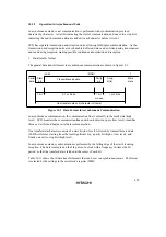
When SCI3 operates on an internal clock, the clock can be output at the SCK
3x
pin. In this case
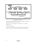
the frequency of the output clock is the same as the bit rate, and the phase is such that the clock
rises at the center of each bit of transmit/receive data, as shown in figure 10.4.
1 character (1 frame)
0
D0
D1
D2
D3
D4
D5
D6
D7
0/1
1
1
Clock
Serial
data
Figure 10.4 Phase Relationship between Output Clock and Transfer Data
(Asynchronous Mode) (8-bit data, parity, 2 stop bits)
3. Data transfer operations
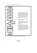
• SCI3 initialization
Before data is transferred on SCI3, bits TE and RE in SCR3 must first be cleared to 0, and then
SCI3 must be initialized as follows.
Note:
If the operation mode or data transfer format is changed, bits TE and RE must first be
cleared to 0.
When bit TE is cleared to 0, bit TDRE is set to 1.
Note that the RDRF, PER, FER, and OER flags and the contents of RDR are retained
when RE is cleared to 0.
When an external clock is used in asynchronous mode, the clock should not be stopped
during operation, including initialization. When an external clock is used in synchronous
mode, the clock should not be supplied during operation, including initialization.


