278
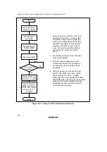
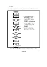
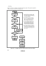
Figure 10.5 shows an example of a flowchart for initializing SCI3.
Start
End
Clear bits TE and
RE to 0 in SCR3
1
2
3
Set bits CKE1
and CKE0
Set data transfer
format in SMR
Set bits SPC31 and
SPC32 to 1 in SPCR
Set value in BRR
No
Wait
Yes
4
Set bits TIE, RIE,
MPIE, and TEIE in
SCR3, and set bits
RE and TE to 1
in PMR7
Has 1-bit period
elapsed?
Set clock selection in SCR3. Be sure to
clear the other bits to 0. If clock output
is selected in asynchronous mode, the
clock is output immediately after setting
bits CKE1 and CKE0. If clock output is
selected for reception in synchronous
mode, the clock is output immediately
after bits CKE1, CKE0, and RE are
set to 1.
Set the data transfer format in the serial
mode register (SMR).
Write the value corresponding to the
transfer rate in BRR. This operation is
not necessary when an external clock
is selected.
Wait for at least one bit period, then set
bits TIE, RIE, MPIE, and TEIE in SCR3,
and set bits RE and TE to 1 in PMR7.
Setting bits TE and RE enables the TXD3x
and RXD3x pins to be used. In asynchronous
mode the mark state is established when
transmitting, and the idle state waiting for
a start bit when receiving.
1.
2.
3.
4.
Figure 10.5 Example of SCI3 Initialization Flowchart


