331
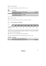
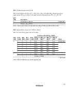
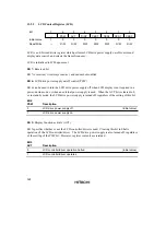
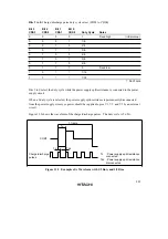
Bits 3 to 0: Charge/discharge pulse duty cycle select (CDS3 to CDS0)
Bit 3
CDS3
Bit 2
CDS2
Bit 1
CDS1
Bit 0
CDS0
Duty Cycle
Notes
0
0
0
0
1
Fixed high
(initial value)
0
0
0
1
1/8
0
0
1
0
2/8
0
0
1
1
3/8
0
1
0
0
4/8
0
1
0
1
5/8
0
1
1
0
6/8
0
1
1
1
0
Fixed low
1
0
*
*
1/16
1
1
*
*
1/32
*
: Don’t care
Bits 3 to 0 select the duty cycle while the power supply split-resistance is connected to the power
supply circuit.
When a 0 duty cycle is selected, the power supply split-resistance is permanently disconnected
from the power supply circuit, so power should be supplied to pins V1, V2, and V3 by an external
circuit.
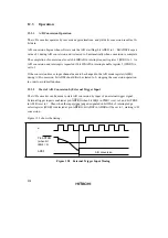
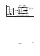
Figure 13.2 shows the waveform of the charge/discharge pulses. The duty cycle is Tc/Tw.
COM1
Charge/discharge
pulses
Tc
Tdc
T
W
1 frame
Tc
Tdc
: Power supply split-resistance
connected
: Power supply split-resistance
disconnected
Figure 13.2 Example of A Waveform with 1/2 Duty and 1/2 Bias

