285
1. Data transfer format
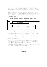
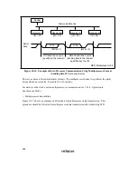
The general data transfer format in asynchronous communication is shown in figure 10.10.
Serial
clock
Serial
data
Note:
*
High level except in continuous transmission/reception
LSB
MSB
*
*
Bit 1
Bit 0
Bit 2
Bit 3
Bit 4
8 bits
One transfer data unit (character or frame)
Bit 5
Bit 6
Bit 7
Don't
care
Don't
care
Figure 10.10 Data Format in Synchronous Communication
In synchronous communication, data on the communication line is output from one falling edge of
the serial clock until the next falling edge. Data confirmation is guaranteed at the rising edge of
the serial clock.
One transfer data character begins with the LSB and ends with the MSB. After output of the
MSB, the communication line retains the MSB state.
When receiving in synchronous mode, SCI3 latches receive data at the rising edge of the serial
clock.
The data transfer format uses a fixed 8-bit data length.
Parity and multiprocessor bits cannot be added.
2. Clock
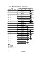
Either an internal clock generated by the baud rate generator or an external clock input at the
SCK
3x
pin can be selected as the SCI3 serial clock. The selection is made by means of bit COM
in SMR and bits CKE1 and CKE0 in SCR3. See table 10.9 for details on clock source selection.
When SCI3 operates on an internal clock, the serial clock is output at the SCK
3x
pin. Eight pulses
of the serial clock are output in transmission or reception of one character, and when SCI3 is not
transmitting or receiving, the clock is fixed at the high level.


