172
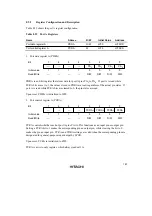
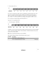
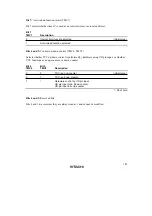
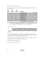
Bit 2: RXD
32
pin input data inversion switch
Bit 2 specifies whether or not RXD
32
pin input data is to be inverted.
Bit 2
SCINV2
Description
0
RXD
32
input data is not inverted
(initial value)
1
RXD
32
input data is inverted
Bit 3: TXD
32
pin output data inversion switch
Bit 3 specifies whether or not TXD
32
pin output data is to be inverted.
Bit 3
SCINV3
Description
0
TXD
32
output data is not inverted
(initial value)
1
TXD
32
output data is inverted
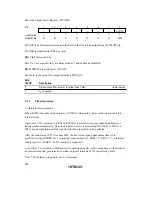
Bit 4: P3
5
/TXD
31
pin function switch (SPC31)
This bit selects whether pin P3
5
/TXD
31
is used as P3
5
or as TXD
31
.
Bit 4
SPC31
Description
0
Functions as P3
5
I/O pin
(initial value)
1
Functions as TXD
31
output pin
*
Note:
*
Set the TE bit in SCR3 after setting this bit to 1.
Bit 5: P4
2
/TXD
32
pin function switch (SPC32)
This bit selects whether pin P4
2
/TXD
32
is used as P4
2
or as TXD
32
.
Bit 5
SPC32
Description
0
Functions as P4
2
I/O pin
(initial value)
1
Functions as TXD
32
output pin
*
Note:
*
Set the TE bit in SCR3 after setting this bit to 1.
Bits 7 and 6: Reserved bits
Bits 7 and 6 are reserved; they are always read as 1 and cannot be modified.


