170
8.10.2
Register Configuration and Description
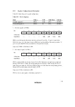
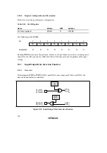
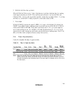
Table 8.26 shows the port B register configuration.
Table 8.26
Port B Register
Name
Abbrev.
R/W
Address
Port data register B
PDRB
R
H'FFDE
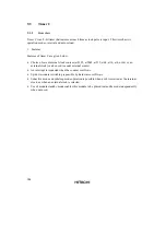
Port Data Register B (PDRB)
Bit
Read/Write
7
PB
R
6
PB
R
5
PB
R
4
PB
R
3
PB
R
0
PB
R
2
PB
R
1
PB
R
3
2
1
0
7
6
5
4
Reading PDRB always gives the pin states. However, if a port B pin is selected as an analog input
channel for the A/D converter by AMR bits CH3 to CH0, that pin reads 0 regardless of the input
voltage.
8.11
Input/Output Data Inversion Function
8.11.1
Overview
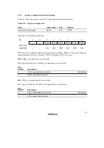
With input pins
WKP
0
to
WKP
7
, RXD
31
, and RXD
32
, and output pins TXD
31
and TXD
32
, the
data can be handled in inverted form.
SCINV0
SCINV2
RXD
31
RXD
32
P3
4
/RXD
31
P4
1
/RXD
32
SCINV1
SCINV3
TXD
31
TXD
32
P3
5
/TXD
31
P4
2
/TXD
32
Figure 8.10 Input/Output Data Inversion Function


