


3.10.1.2 Port control and interrupt summary
The following table provides more information regarding the Port Control and Interrupt
configurations .
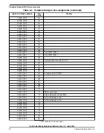
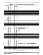
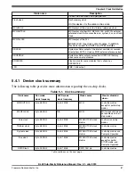
Table 3-38. Ports summary
Feature
Port A
Port B
Pull select control
No
No
Pull select at reset
PTA0=Pull down, Others=Pull up
Pull up
Pull enable control
Yes
Yes
Pull enable at reset
PTA0/PTA2/RESET_b=Enabled;
Others=Disabled
PTB5=Enabled; Others=Disabled
Slew rate enable control
No
No
Slew rate enable at reset
PTA2/PTA6/PTA7=Disabled;
Others=Enabled
PTB0= Disabled; Others=Enabled
Passive filter enable control
RESET_b only
PTB5 only
Passive filter enable at reset
RESET_b=Enabled; Others=Disabled
Disabled
Open drain enable control
No
No
Open drain enable at reset
Disabled
Disabled
Drive strength enable control
PTA12/PTA13 only
PTB0/PTB1 only
Drive strength enable at reset
Disabled
Disabled
Pin mux control
Yes
Yes
Pin mux at reset
PTA0/PTA2=ALT3; Others=ALT0
PTB5=ALT3; Others=ALT0
Lock bit
No
No
Interrupt request
PTA0/PTA1/PTA7/PTA10/PTA11/PTA12
only
PTB0/PTB1/PTB2/PTB3/PTB4/PTB5/
PTB6/PTB7 only
Digital glitch filter
No
No
1. UART signals can be configured for open-drain using SIM_SOPT5 register. IIC signals are automatically enabled for open
drain when selected.
3.10.1.3 GPIO accessibility in the memory map
The GPIO is multi-ported and can be accessed directly by the core with zero wait states at
base address 0xF800_0000. It can also be accessed by the core through the cross bar/
AIPS interface at 0x400F_F000 and at an aliased slot (15) at address 0x4000_F000. All
BME operations to the GPIO space can be accomplished referencing the aliased slot (15)
at address 0x4000_F000. Only some of the BME operations can be accomplished
referencing GPIO at address 0x400F_F000.
Chapter 3 Chip Configuration
KL02 Sub-Family Reference Manual, Rev. 2.1, July 2013
Freescale Semiconductor, Inc.
75


