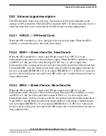


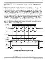


SS OUT
SS IN
(SLAVE)
(MASTER)
(SLAVE OUT)
MISO
MSB FIRST
LSB FIRST
MOSI
(MASTER OUT)
(MISO OR MOSI)
SAMPLE IN
SPSCK
(CPOL = 1)
SPSCK
(CPOL = 0)
BIT TIME #
(REFERENCE)
BIT 7
BIT 0
BIT 6
BIT 1
BIT 2
BIT 5
BIT 0
BIT 7
BIT 1
BIT 6
1
2
6
7
8
...
...
...
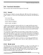
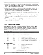
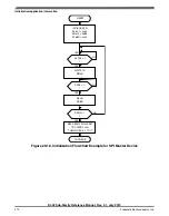
Figure 29-15. SPI clock formats (CPHA = 1)
When C1[CPHA] = 1, the slave begins to drive its MISO output when SS goes to active
low, but the data is not defined until the first SPSCK edge. The first SPSCK edge shifts
the first bit of data from the shifter onto the MOSI output of the master and the MISO
output of the slave. The next SPSCK edge causes both the master and the slave to sample
the data bit values on their MISO and MOSI inputs, respectively. At the third SPSCK
edge, the SPI shifter shifts one bit position which shifts in the bit value that was just
sampled, and shifts the second data bit value out the other end of the shifter to the MOSI
and MISO outputs of the master and slave, respectively.
When C1[CPHA] = 1, the slave's SS input is not required to go to its inactive high level
between transfers. In this clock format, a back-to-back transmission can occur, as
follows:
1. A transmission is in progress.
2. A new data byte is written to the transmit buffer before the in-progress transmission
is complete.
3. When the in-progress transmission is complete, the new, ready data byte is
transmitted immediately.
Chapter 29 Serial Peripheral Interface (SPI)
KL02 Sub-Family Reference Manual, Rev. 2.1, July 2013
Freescale Semiconductor, Inc.
459


