
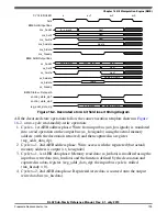
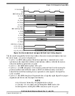
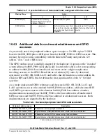

NOTE
Any wait states inserted by the peripheral slave device
(sx_hready = 0) are simply passed through the BME back to the
master input bus, stalling the AHB transaction cycle for cycle.
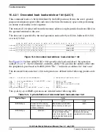
16.4.1.1 Decorated store logical AND (AND)
This command performs an atomic read-modify-write of the referenced memory location.
1. First, the location is read;
2. It is then modified by performing a logical AND operation using the write data
operand sourced for the system bus cycle
3. Finally, the result of the AND operation is written back into the referenced memory
location.
The data size is specified by the write operation and can be byte (8-bit), halfword (16-bit)
or word (32-bit). The core performs the required write data lane replication on byte and
halfword transfers.
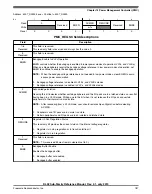
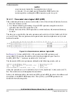
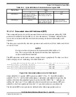
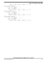
31 30 29 28 27 26 25 24 23 22 21 20 19 18 17 16 15 14 13 12 11 10
9
8
7
6
5
4
3
2
1
0
ioandb
0 1 0 0 0 1
-
-
-
-
-
-
mem_addr
ioandh
0 1 0 0 0 1
-
-
-
-
-
-
mem_addr
0
ioandw
0 1 0 0 0 1
-
-
-
-
-
-
mem_addr
0 0
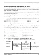
Figure 16-3. Decorated store address: logical AND
See
where addr[28:26] = 001 specifies the AND operation, and
mem_addr[19:0] specifies the address offset into the peripheral space based at
0x4000_0000. The "-" indicates an address bit "don't care".
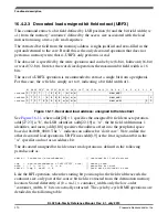
The decorated AND write operation is defined in the following pseudo-code as:
ioand<sz>(accessAddress, wdata) // decorated store AND
tmp = mem[accessAddress & 0xE00FFFFF, size] // memory read
tmp = tmp & wdata // modify
mem[accessAddress & 0xE00FFFFF, size] = tmp // memory write
where the operand size <sz> is defined as b(yte, 8-bit), h(alfword, 16-bit) and w(ord, 32-
bit). This notation is used throughout the document.
In the cycle definition tables, the notations AHB_ap and AHB_dp refer to the address and
data phases of the BME AHB transaction. The cycle-by-cycle BME operations are
detailed in the following table.
Functional description
KL02 Sub-Family Reference Manual, Rev. 2.1, July 2013
200
Freescale Semiconductor, Inc.


