


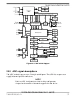
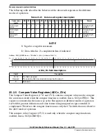

Table 25-1. ADC signal descriptions
Signal
Description
I/O
AD
n
Single-Ended Analog Channel Inputs
I
V
DDA
Analog Power Supply
I
V
SSA
Analog Ground
I
25.2.1 Analog Power (V
DDA
)
The ADC analog portion uses V
DDA
as its power connection. In some packages, V
DDA
is
connected internally to V
DD
. If externally available, connect the V
DDA
pin to the same
voltage potential as V
DD
. External filtering may be necessary to ensure clean V
DDA
for
good results.
25.2.2 Analog Ground (V
SSA
)
The ADC analog portion uses V
SSA
as its ground connection. In some packages, V
SSA
is
connected internally to V
SS
. If externally available, connect the V
SSA
pin to the same
voltage potential as V
SS
.
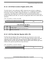
25.2.3 Analog Channel Inputs (ADx)
The ADC module supports up to 24 single-ended analog inputs. A single-ended input is
selected for conversion through the SC1[ADCH] channel select bits.
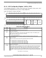
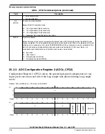
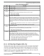
25.3 Memory map and register definitions
This section describes the ADC registers.
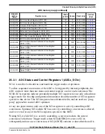
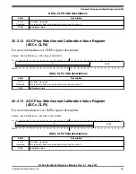
ADC memory map
Absolute
address
(hex)
Register name
Width
(in bits)
Access Reset value
Section/
page
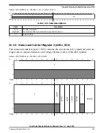
4003_B000 ADC Status and Control Registers 1 (ADC0_SC1A)
32
R/W
0000_001Fh
4003_B004 ADC Status and Control Registers 1 (ADC0_SC1B)
32
R/W
0000_001Fh
4003_B008 ADC Configuration Register 1 (ADC0_CFG1)
32
R/W
0000_0000h
4003_B00C ADC Configuration Register 2 (ADC0_CFG2)
32
R/W
0000_0000h
Table continues on the next page...
Memory map and register definitions
KL02 Sub-Family Reference Manual, Rev. 2.1, July 2013
342
Freescale Semiconductor, Inc.


