


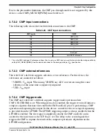


Signal multiplexing
Module signals
Register
access
CMP
Peripheral
bridge 0
Other peripherals
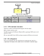
Figure 3-19. CMP configuration
Table 3-28. Reference links to related information
Topic
Related module
Reference
Full description
Comparator (CMP)
System memory map
—
Clocking
—
Power management
—
Signal multiplexing
Port control
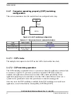
3.7.2.1 CMP instantiation information
The device includes one high-speed comparator and two 8-input multiplexers for both the
inverting and non-inverting inputs of the comparator. Each CMP input channel connects
to both muxes. Two of the channels are connected to internal sources, leaving resources
to support up to 6 input pins. See the channel assignment table for a summary of CMP
input connections for this device.
The CMP also includes one 6-bit DAC with a 64-tap resistor ladder network, which
provides a selectable voltage reference for applications where voltage reference is needed
for internal connection to the CMP.
The CMP can be optionally on in all modes except VLLS0.
The CMP has several module-to-module interconnects in order to facilitate ADC
triggering, TPM triggering, and UART IR interfaces. For complete details on the CMP
module interconnects, see the
The CMP does not support window compare function and a 0 must always be written to
CMP_CR1[WE]. The sample function has limited functionality since the SAMPLE input
to the block is not connected to a valid input. Usage of sample operation is limited to a
divided version of the bus clock (CMP_CR1[SE] = 0).
Analog
KL02 Sub-Family Reference Manual, Rev. 2.1, July 2013
64
Freescale Semiconductor, Inc.


