


Table 10-13. I
2
C1 Signal Descriptions
Chip signal name
Module signal
name
Description
I/O
I2C1_SCL
SCL
Bidirectional serial clock line of the I
2
C system.
I/O
I2C1_SDA
SDA
Bidirectional serial data line of the I
2
C system.
I/O
Table 10-14. UART0 signal descriptions
Chip signal name
Module signal
name
Description
I/O
UART0_TX
TxD
Transmit data
O
UART0_RX
RxD
Receive data
I
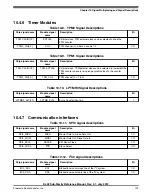
10.4.8 Human-machine interfaces (HMI)
Table 10-15. GPIO Signal Descriptions
Chip signal name
Module signal
name
Description
I/O
PTA[31:0]
PORTA31–PORTA0 General-purpose input/output
I/O
PTB[31:0]
PORTB31–PORTB0 General-purpose input/output
I/O
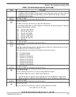
1. The available GPIO pins depend on the specific package. See the signal multiplexing section for which exact GPIO signals
are available.
Module Signal Description Tables
KL02 Sub-Family Reference Manual, Rev. 2.1, July 2013
130
Freescale Semiconductor, Inc.


