


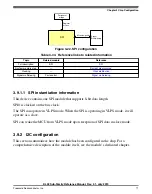
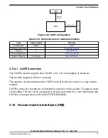


Signal
multiplexing
Register
access
SPI
Peripheral
bridge
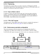
Module signals
Figure 3-22. SPI configuration
Table 3-34. Reference links to related information
Topic
Related module
Reference
Full description
SPI
System memory map
—
Clocking
—
Signal multiplexing
Port control
3.9.1.1 SPI instantiation information
This device contains one SPI module that supports 8-bit data length.
SPI0 is clocked on the bus clock.
The SPI can operate in VLPS mode. When the SPI is operating in VLPS mode, it will
operate as a slave.
SPI can wake the MCU from VLPS mode upon reception of SPI data in slave mode.
3.9.2 I2C configuration
This section summarizes how the module has been configured in the chip. For a
comprehensive description of the module itself, see the module’s dedicated chapter.
Chapter 3 Chip Configuration
KL02 Sub-Family Reference Manual, Rev. 2.1, July 2013
Freescale Semiconductor, Inc.
71


