


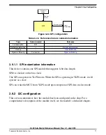


3.10.1 GPIO configuration
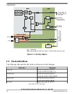
Signal multiplexing
Register
access
Peripheral
bridge
Module signals
GPIO controller
ARM Cortex -M0+
Core
Register access
Figure 3-25. GPIO configuration
Table 3-37. Reference links to related information
Topic
Related module
Reference
Full description
GPIO
System memory map
—
Clocking
—
Power management
—
Crossbar switch
Crossbar switch
Signal multiplexing
Port control
3.10.1.1 GPIO instantiation information
The device includes four pins, PTB0, PTB1, PTA12, and PTA13, with high current drive
capability. These pins can be used to drive LED or power MOSFET directly. The high
drive capability applies to all functions which are multiplexed on these pins (UART,
TPM, SPI...etc)
The device includes two pins, PTB3 and PTB4, with true open drain setting. These pins
have the capability to support 5 V voltage input in 3.3 V systems.
3.10.1.1.1 Pull devices and directions
The pull devices are enabled out of POR only on RESET_b, NMI_b and respective SWD
signals. Other pins can be enabled by writing to PORTx_PCRn[PE].
All the pins are hard wired to be pullup except for SWD_CLK. The state will be reflected
in the PORTx_PCRn[PS] field.
Human-machine interfaces (HMI)
KL02 Sub-Family Reference Manual, Rev. 2.1, July 2013
74
Freescale Semiconductor, Inc.


