C
URTISS
-W
RIGHT
P
RODUCT
O
VERVIEW
826448 V
ERSION
5 M
ARCH
2015
P
ROPRIETARY
1-15
N
ON
-V
OLATILE
RAM (NVRAM)
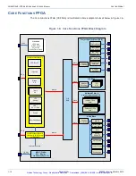
A 256KB non-volatile memory device based on ferro-electric technology (F-RAM) provides
non-volatile storage of mission state data that must be preserved when power is removed.
During normal operation, application software views the NVRAM like a standard SRAM, except
that data is retained after power is removed. A serial interface NVRAM is used on the
CHAMP-AV8, accessible via API functions. Both processors have access to the NVRAM device
via the Core Functions FPGA. Data written to the NVRAM is immediately non-volatile.
The device is rated for a minimum of 100 Trillion (10
14
) read/write cycles. The data retention
period is >10 years. For security against inadvertent writes to NVRAM, a hardware
write-protection feature is provided (jumper, JB6) – see Table 2.3, “Jumper Block Definition,”
on page 2-7 for more details.
N
ON
-V
OLATILE
M
EMORY
S
ECURITY
The CHAMP-AV8, as well as other Curtiss-Wright Controls Continuum Architecture products,
provides for the management of non-volatile memory devices in classified circumstances. All
of the non-volatile devices, boot flash, backup boot flash, NAND flash, NVRAM and FPGA PROM
may be write-protected by hardware jumpers. The jumpers may be visually inspected to
conform to security procedures. The firmware of the CHAMP-AV8 provides a non-volatile
memory scrub function to perform a secure erase per NISPOM requirements. See Appendix B,
"Statement of Memory Volatility" for details of memory devices present on the CHAMP-AV8.
XMC S
ITE
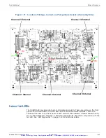
The CHAMP-AV8 is equipped with one XMC site, as a build option, that provides additional user
I/O on a P14 connector. This site complies with ANSI/VITA 42.0 and ANSI/VITA 42.3.
The CHAMP-AV8 uses a 10 mm XMC stacking height.
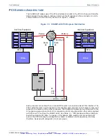
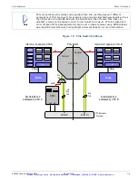
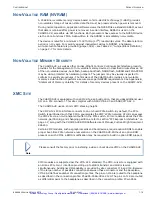
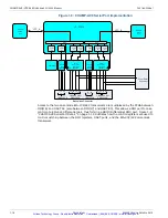
The XMC site's PCIe interface connects to an on-board PCIe Switch. By default, the PCIe
Switch is partitioned such that CPU A enumerates the XMC's PCIe network. CPU B can access
the XMC site via a non-transparent buffer in the PCIe switch. For more details about the PCIe
network, partitioning, and changing partitions, refer to section “PCI Express Architecture” on
page 1-7, along with the CHAMP-AV8 BIOS Software User's Manual, Curtiss-Wright document
826450.
Certain XMC modules, such as graphics cards and boot devices, require option ROMs to enable
proper boot-time PCIe network enumeration on the CHAMP-AV8. Without an option ROM
present on such XMCs, a BIOS modification may be required to build in option ROM support.
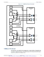
XMC modules are supported per the VITA 42.3 standard. The XMC-only site is equipped with
an 8-lane PCIe Gen 1 interface providing up to 2GB/s transmit and 2GB/s receive
simultaneously. Additional I/O capability is provided by site connectors J16 and J14. Because
of the large number of possible connections between these connectors and the backplane,
VITA 46.9 defines a number of connection profiles. The pins on J16 are routed to the backplane
as described in the connection profile: P5w3P6-X38s+X8d+X12d. The pins on J14 are routed
as differential pairs to the backplane as described in the connection profile: P3w1-P64s.
Note
Please consult the factory prior to installing a video or boot device XMC on the CHAMP-AV8.
Artisan Technology Group - Quality Instrumentation ... Guaranteed | (888) 88-SOURCE | www.artisantg.com


