C
URTISS
-W
RIGHT
1
826448 V
ERSION
5 M
ARCH
2015
P
ROPRIETARY
A-5
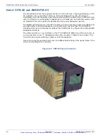
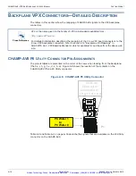
With reference to Figure A.3 below, four types of wafers are used, including power, single
ended, or differential (with odd or even routing configurations). The P0 through P6 connectors
on the CHAMP-AV8 employ these different wafer types in specific combinations to meet the
requirements of the interface.
Figure A.3: VPX RT2 Wafer Routings
Connector Wafer
Plug-in Module PWB
B
a
ckpl
ane PW
B
Plug-in Row
A
B
C
D
E
F
G
Ba
ckplane
Row
i
h
g
f
e
d
c
b
a
GND
hx
gx
GND
ex
GND
cx
bx
GND
fx
GND
ix
GND
dx
GND
ax
GND
hx
gx
ex
cx
bx
Sig 5
to hx
Sig 4
to
g
x
Sig 3
to ex
Sig 2
to
c
x
Sig 1
to bx
Single-Ended Plug-in Module Wafer to Backplane Routings P0-J0
Power Wafer to Backplane Routings P0-J0
Connector Wafer
B
a
ckpl
a
ne PWB
Ba
ckplane
Row
i
h
g
f
e
d
c
b
a
hx
gx
cx
dx
gx
cx
Pwr 2
to
f,
g
, h
, i
x
Pwr 1
to
a, b,
c,
dx
bx
fx
hx
ix
Plug-in Module PWB
Plug-in Row
A
B
C
D
G
E
F
ax
ax
bx
ex
fx
ix
dx
Differential Plug-in Module Wafer to Backplane Routings – Even Wafers
Connector Wafer
B
a
ckpl
ane PW
B
Ba
ckplane
Row
i
h
g
f
e
d
c
b
a
GND
hx
gx
GND
GND
cx
dx
GND
GND
GND
dx
GND
GND
gx
cx
Pair 2
to
h
x
to gx
Pair 1
to
d
x
bx
to cx
ex
fx
hx
ix
Plug-in Module PWB
Plug-in Row
A
B
C
D
G
E
F
GND
GND
ax
Differential Plug-in Module Wafer to Backplane Routings – Odd Wafers
Connector Wafer
B
a
ckpl
ane PW
B
Ba
ckplane
Row
i
h
g
f
e
d
c
b
a
GND
ix
fx
GND
ex
GND
ax
bx
GND
GND
GND
dx
GND
GND
gx
cx
Single Ended 1
to i
x
Pair 2
to
fx
to ex
Pair 1
to
b
x
bx
to ax
ax
ex
fx
hx
ix
Plug-in Module PWB
Plug-in Row
A
B
C
D
G
E
F
Artisan Technology Group - Quality Instrumentation ... Guaranteed | (888) 88-SOURCE | www.artisantg.com


