background image

C

URTISS

-W

RIGHT

P

RE

-I

NSTALLATION

 T

ASKS

826448 V

ERSION

 5 M

ARCH

 2015

P

ROPRIETARY

2-5

The XMC site provides traditional PMC I/O, single ended XMC I/O, and high-speed differential 
XMC I/O. The traditional PMC I/O consists of 64 bits of I/O that are differentially routed 
between the XMC J14 connector and the CHAMP-AV8 backplane P3 connector.

The CHAMP-AV8 utilizes a 10 mm XMC stacking height.

Mezzanine Module 
Power 
Considerations

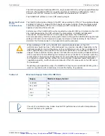
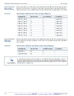
The CHAMP-AV8 supplies voltages to the XMC site according to VITA 42. The supplied voltages 
are listed in Table 2.2, along with their maximum supply currents. These maximum supply 
currents are specified by VITA 42 at 1 Ampere per XMC connector pin. The CHAMP-AV8 is 
capable of providing these currents.

Performance of the CHAMP-AV8 may be impacted by a specific XMC card installed on the XMC 
site. Heat dissipated by the XMC will raise the temperature of CHAMP-AV8 basecard 
components. At elevated inlet air or card edge temperature, the CHAMP-AV8's 
microprocessors may throttle, reducing performance. Although the CHAMP-AV8 supports high 
wattage XMC cards and is designed to supply maximum current according to the VITA 42 
standard, the thermal impact on the basecard should be assessed.

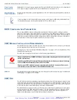
Caution

When installing an XMC on the CHAMP-AV8, careful characterization of the XMC 
performance should be done. Technical Support may also be consulted. Depending on the 
particular application and configuration, various conditions can occur that could adversely 
affect (and possibly extend oustide of the product specification) the baseboard, XMC, or 
chassis. These conditions include, but are not limited to excessive heating of baseboard and 
XMC components. Factors affecting this include, but are not limited to: maximum operating 
temperature of the board (air temperature for air-cooled boards and card edge temperature 
for conduction-cooled boards), airflow (air-cooled boards), baseboard power dissipation 
(application specific), and the location and density of the hot components on the XMC and/or 
the baseboard.

Depending upon application usage, the CHAMP-AV8 may require operational derating when 
used in conjunction with a mezzanine. Consult the factory for guidance.

Table 2.2:

Maximum Supply Current for XMC Site

Supply

Maximum Supply Current

12 VPWR

8A

3.3V_AUX

1A

3.3V

4A

+12V

1A

-12V

1A

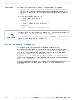
Note

The use of a mezzanine may induce lowered CPU performance at elevated temperatures. 
Consult the factory for guidance. 

Artisan Technology Group - Quality Instrumentation ... Guaranteed | (888) 88-SOURCE | www.artisantg.com

Summary of Contents for CHAMP-AV8

Page 1: ...l service in house repair center WE BUY USED EQUIPMENT Sell your excess underutilized and idle used equipment We also offer credit for buy backs and trade ins www artisantg com WeBuyEquipment REMOTE INSPECTION Remotely inspect equipment before purchasing with our interactive website at www instraview com LOOKING FOR MORE INFORMATION Visit us on the web at www artisantg com for more information on ...

Page 2: ...ent is the property of Curtiss Wright Controls Inc CW Controls and shall not be copied or used in whole or in part without prior written permission from CW Controls CHAMP AV8 VPX6 462 VPX QUAD CORE INTEL CORE i7 DSP BOARD HARDWARE USER S MANUAL 826448 5 March 2015 Artisan Technology Group Quality Instrumentation Guaranteed 888 88 SOURCE www artisantg com ...

Page 3: ...on on page 3 4 Replaced Figure 3 2 System Boot Screen on page 3 11 Updated section Display the Initial Screen Message on page 3 13 Replaced Figure 3 3 GRUB Loading Message on page 3 13 Updated section Troubleshooting on page 3 14 Updated Table 3 7 Summary of LED Behavior on page 3 15 Updated Appendix A Connector Pin Assignments Added Appendix B Statement of Memory Volatility Added Appendix C Memor...

Page 4: ...ctions on page 1 26 Updated Table 1 4 VPX Compliance Summary on page 1 31 Updated Table 1 11 Summary of CHAMP AV8 Connectors Functions Supported on page 1 39 Updated Continuum IPC Library on page 1 40 Updated Continuum Vector Library on page 1 41 Updated Backplane Requirements on page 2 2 Updated Detailed Power Requirements on page 2 3 Updated XMC Site on page 2 4 Removed the caution note in Insta...

Page 5: ... Wright Controls Inc The acceptance of this document will be construed as an acceptance of the foregoing condition Copyright 2015 Curtiss Wright Controls Inc All rights reserved TRADEMARKS Adobe and Acrobat are trademarks of Adobe Systems Incorporated Ethernet is a trademark of Xerox Corporation Fedora is a trademark of Red Hat Inc Intel and Intel Core are trademarks or registered trademarks of In...

Page 6: ...imers 1 16 Avionics Style Watchdog Timer 1 16 Multi board Synchronous Clock 1 17 Serial Ports 1 17 1000Base T Ethernet 1 19 1000Base BX Ethernet 1 20 USB and SATA Interfaces 1 20 LVTTL Discrete Digital I O 1 21 EIA 422 Differential Discrete Digital I O 1 21 Voltage Current and Temperature Sensors 1 22 Indicator LEDs 1 23 Cables and Rear Transition Modules 1 24 RTC CMOS RAM Backup Power 1 24 Interr...

Page 7: ... 3 11 Initiate the Power Up Sequence 3 12 Display the Initial Screen Message 3 13 Troubleshooting 3 14 Verify Insertion in Chassis 3 14 LED Diagnostics 3 14 LED Start Up Sequence Power On 3 19 LED Start Up Sequence Reset 3 20 Sign on Message Garbled 3 20 The Next Step 3 20 A Connector Pin Assignments A 1 In This Appendix A 1 Connector Overview A 3 Backplane VPX Connectors A 3 About VITA 46 and ANS...

Page 8: ...J6 XMC DIO SATA USB Connector Pin Assignments A 35 J1 Front Panel Connector A 36 XMC Site s PMC J14 Connector A 39 XMC Site s PMC J14 User I O Connector A 39 XMC J15 and J16 Connectors A 42 XMC J15 Connector A 42 XMC J16 User I O Connector A 45 Rear Transition Module RTM A 52 Rear Transition Module Panel Mounted Connectors A 54 Rear Transition Module RTM Configuration Switches A 57 Rear Transition...

Page 9: ...CHAMP AV8 VPX6 462 HARDWARE USER S MANUAL CURTISS WRIGHT VIII PROPRIETARY 826448 VERSION 5 MARCH 2015 Artisan Technology Group Quality Instrumentation Guaranteed 888 88 SOURCE www artisantg com ...

Page 10: ... 8 Figure 3 1 Location of CHAMP AV8 Ethernet Activity LEDs 3 7 Figure 3 2 System Boot Screen 3 11 Figure 3 3 GRUB Loading Message 3 13 Figure A 1 VPX System Connectors Overview A 3 Figure A 2 VPX RT2 Type Connector A 4 Figure A 3 VPX RT2 Wafer Routings A 5 Figure A 4 CHAMP AV8 Backplane P0 P6 Connector Orientation A 7 Figure A 5 I O Mapping to the CHAMP AV8 VITA 46 Connectors A 8 Figure A 6 CHAMP ...

Page 11: ...CHAMP AV8 VPX6 462 HARDWARE USER S MANUAL CURTISS WRIGHT X PROPRIETARY 826448 VERSION 5 MARCH 2015 Artisan Technology Group Quality Instrumentation Guaranteed 888 88 SOURCE www artisantg com ...

Page 12: ...ignal Definitions A 18 Table A 8 VPX Backplane J1 Pin Assignments A 19 Table A 9 P2 PCIe Expansion Plane Connector Pin Assignments A 21 Table A 10 P2 PCIe Expansion Plane Connector Signal Definitions A 21 Table A 11 VPX Backplane J2 Pin Assignments A 22 Table A 12 P3 XMC Site s PMC User I O Connector Pin Assignments A 24 Table A 13 P3 XMC Site s PMC User I O Connector Signal Definitions A 24 Table...

Page 13: ... SW18 Functions A 57 Table A 40 RTM Header Functions A 58 Table A 41 RTM PMC I O JB2 Pin Assignments A 59 Table A 42 RTM Discrete I O P4 P5 Pin Assignments A 61 Table A 43 RTM Geographical Address P12 Pin Assignments A 61 Table A 44 XMC Single Ended I O JB6 Pin Assignments A 62 Table A 45 RTM XMC Differential User I O J7 Pin Assignments A 63 Table B 1 Memory Devices Available On The CHAMP AV8 B 2 ...

Page 14: ...view of the features and functions of the CHAMP AV8 product This includes a technical description and a block diagram Chapter 2 Pre Installation Tasks This chapter discusses tasks that must be performed before installing the CHAMP AV8 in a system including checking power requirements Chapter 3 Hardware Installation This chapter explains how to install the CHAMP AV8 into a VPX chassis and verify th...

Page 15: ...fic hardware configuration of your particular variant CHAMP AV8 Product Release Notes 8xxxxx CHAMP AV8 VPX Quad core Core i7 DSP Board BIOS Release Notes 826451 Contents information about the most recent CHAMP AV8 BIOS release CHAMP AV8 VPX Quad core Core i7 DSP Board VxWorks BSP Software User s Manual 826452 Contents BSP overview BSP installation instructions Memory maps usage Programming instruc...

Page 16: ...ystem Specifications ANSI VITA 65 2010 PCI Express Base Specification Revision 2 1 March 4 2009 PCI SIG Interface Between Data Terminal Equipment and Data Circuit Terminating Equipment Employing Serial Binary Data Interchange ANSI TIA EIA 232 F 1997 September 30 1997 RapidIO Interconnect Specification Part IV Physical Layer 1x 4x LP Serial Specifica tion Revision 1 2 June 2002 Interface Between Da...

Page 17: ...to describe the size of a memory device or a range of addresses Table 1 Typographic Conventions Item Convention Example Keystrokes Keys are listed as they appear on most keyboards surrounded by marks Combinations of key strokes appear within a single set of brackets Type Ctrl Alt C to return to the previous menu Type Esc to exit File Names File names are set in italics Copy the file named bootA ex...

Page 18: ...IO Discrete Input Output DMA Direct Memory Access DVT Design Verification Test ECC Error Correction Code EEPROM Electrically Erasable Programmable Read Only Memory EIA Electronic Industries Association EMI Electro Magnetic Interference EPROM Erasable Programmable Read Only Memory FPGA Field Programmable Gate Array GND Ground GPIO General Purpose Input Output HUM Hardware User s Manual I F Interfac...

Page 19: ...e PCI Express PCISIG PCI Special Interest Group PICMG PCI Industrial Computer Manufactures Group PMC PCI Mezzanine Card PROM Programmable Read Only Memory PSB Processor Specific Block PWB Printed Wiring Board RAM Random Access Memory RTM Rear Transition Module SATA Serial ATA SDRAM Synchronous Dynamic RAM memory SHMUART Shared Memory UART SPI Serial Peripheral Interface SRAM Static Random Access M...

Page 20: ...ial information Caution This is a caution The caution icon indicates non catastrophic incidents complex practices or procedures which if not observed could result in damage to the hardware Cautions include specific instructions for avoiding or minimizing these incidents Warning This is a warning The warning icon indicates procedures in the manual that if not carried out or if carried out incorrect...

Page 21: ...ted technical documentation in addition to software components etc as these items become available To Access Curtiss Wright Technical Support For Technical Support and Repair and Warranty services information go to the Curtiss Wright web site http www cwcdefense com and click on the SUPPORT link near the top of the page This will bring up the following web page http www cwcdefense com support html...

Page 22: ... page 1 12 Double Data Rate DDR3 SDRAM with ECC on page 1 13 Protected Boot Flash Memory on page 1 14 NAND Flash Memory on page 1 14 Non Volatile RAM NVRAM on page 1 15 Non Volatile Memory Security on page 1 15 XMC Site on page 1 15 Utility Features Semaphores Timers on page 1 16 Avionics Style Watchdog Timer on page 1 16 Multi board Synchronous Clock on page 1 17 Serial Ports on page 1 17 1000Bas...

Page 23: ...brary on page 1 40 Continuum Vector Library on page 1 41 GENERAL DESCRIPTION The CHAMP AV8 multi processing board brings the floating point performance of the Intel Core i7 architecture to VPX form factor standard Utilizing a pair of second generation Intel i7 2715QE or third generation Intel i7 3612QE quad core processors the CHAMP AV8 delivers up to 269 GFlops of performance The CHAMP AV8 featur...

Page 24: ...UMMARY Two Intel Core i7 second i7 2715QE or third i7 3612QE generation processors running at up to 2 1GHz Hyper threading technology Up to 269 GFlops computing performance 4GB DDR3 SDRAM with ECC per processor FRONT ISOMETRIC REAR ISOMETRIC Artisan Technology Group Quality Instrumentation Guaranteed 888 88 SOURCE www artisantg com ...

Page 25: ...one EIA 422 port always present plus either two EIA 232 ports or one EIA 422 port software configurable Three USB 2 0 interfaces Two eSATA interfaces 16 LVTTL I O signals with interrupt Differential discrete I O 12 general purpose timers Avionics watchdog timer 16 semaphore registers Multi board synchronous clock feature Temperature sensors Voltage and current sensors for measuring power consumpti...

Page 26: ...6 MB Recovery Flash SPI_B Boot Flash 8 or 16 MB Recovery Flash SPI_A Sync Clock Semaphores Watchdog Timers GPIO Security NVRAM 256KB LPC_B Power Temp SPI_B LPC_A SPI_A Node A SDRAM Control SDRAM Control L3 PCIe L1 L2 Core L1 L2 Core L1 L2 Core L1 L2 Core PCIe PCIe Node A SDRAM Control SDRAM Control L3 PCIe L1 L2 Core L1 L2 Core L1 L2 Core L1 L2 Core PCIe PCIe 32 Lane x8 x0 x0 x8 2x4 2 x EIA 422 2 ...

Page 27: ...s With two processors the CHAMP AV8 provides 270 GFlops of performance Featuring a dual channel 1333 MHz DDR3 SDRAM interface each CPU has a peak memory bandwidth of 21GB s The 2nd and 3rd generation Core processors feature many improvements in the cache subsystem designed to increase hit rate and lower latency Each core contains first level instruction and data caches 32 KB 4 way and a second lev...

Page 28: ...orm connections to I O devices and or other cards enabled with PCIe on P2 such as the CHAMP AV8 See Table 1 1 XMC Expansion Plane Interface Build Time Options for PCIe on page 1 8 for details PCIe switch ports connected to P2 and or the XMC site may be configured to enable or disable non transparency and may therefore be used with endpoints or root complexes I O Hub PCIe Switch SDRAM Control SDRAM...

Page 29: ...CHAMP AV8 BIOS Software User s Manual Curtiss Wright document 826450 The default partition is illustrated in Figure 1 4 PCIe Switch Partitions on page 1 9 With this default partition PCIe circuitry on the XMC site or EP 08 15 depending on the build option selected is enumerated by CPU A and cannot be addressed directly from CPU B PCIe circuitry interfaced to EP 00 07 is enumerated by CPU B and can...

Page 30: ...alues using BIOS settings See the BIOS User s Manual Curtiss Wright document 826450 for more information I O Hub I O Hub VPX Backplane Connector DMI x4 DMI x4 XMC Pn4 Intel Core i7 quad core CPU A J6 Node A SDRAM Control SDRAM Control L3 PCIe L1 L2 Core L1 L2 Core L1 L2 Core L1 L2 Core PCIe PCIe Node A SDRAM Control SDRAM Control L3 PCIe L1 L2 Core L1 L2 Core L1 L2 Core L1 L2 Core PCIe PCIe Factor...

Page 31: ...f board SRIO fabric connectivity and enables distributed switching architectures avoiding the need for a separate switch card The PCIe SRIO bridges operate at a SRIO link maximum rate of 5Gbps Multiple CHAMP AV8 cards may be connected using the SRIO fabric interface Table 1 2 below and Figure 1 5 on page 1 11 show the SRIO port numbers and mapping to the processor and the backplane Table 1 2 CPS 1...

Page 32: ...upported on both boards In this case the CHAMP AV8 would be down graded to the Gen 1 speed See the BIOS User s Manual Curtiss Wright document 826450 for more information Node A Intel Core i7 quad core Node A SDRAM Control SDRAM Control L3 PCIe L 1 L2 Core L 1 L2 Core L 1 L2 Core L 1 L2 Core PCIe PCIe P1 Connector PCIe SRIO PCIe SRIO PCIe SRIO PCIe SRIO SRIO Gen2 Switch x4 SRIO Node A SDRAM Control...

Page 33: ...Specific Block PSB SHMUART Block Address Decoding I2C Volt Temp Sensors SPI NVRAM Reset CPLD Ctrl Status Address Decoding Address Decodeing I2O X 4 Slave Inbound FIFOs 8x64 4 sets of In Outbound FIFO Outbound FIFOs 8x64 Slave BOOT FLASH SPI Monitor to observe boot I F PCH SPI I F Slave Utility Block Address Decoding MBSC Misc Ctrl Config Status Config PROM I F DIO Master Clock Gen LPC Clocks MBSC ...

Page 34: ...allows other CPUs in the fabric to communicate directly with the owner Writing to an Inbound Doorbell Register causes an interrupt request to the owner CPU As with the Doorbell Registers there are four 32 bit Inbound Message Queues each with an owner Each queue holds 512 messages The Inbound Post Queue holds posted messages from the fabric to owner CPUs The owner CPU fetches the next message proce...

Page 35: ...ry and secondary boot flash devices feature hardware write protection jumpers JB7 for the primary boot flash and JB5 for the secondary boot flash see Table 2 3 Jumper Block Definition on page 2 7 for more details NAND FLASH MEMORY The CHAMP AV8 features 8 GB of NAND flash per processor 16 GB total per CHAMP AV8 for storage of the operating system and user application software A SATA interface conn...

Page 36: ...MC SITE The CHAMP AV8 is equipped with one XMC site as a build option that provides additional user I O on a P14 connector This site complies with ANSI VITA 42 0 and ANSI VITA 42 3 The CHAMP AV8 uses a 10 mm XMC stacking height The XMC site s PCIe interface connects to an on board PCIe Switch By default the PCIe Switch is partitioned such that CPU A enumerates the XMC s PCIe network CPU B can acce...

Page 37: ...features AVIONICS STYLE WATCHDOG TIMER The CHAMP AV8 provides two watchdog timers for each processor Each watchdog timer is a pre settable down counter with a resolution of 1 µsec Time out periods from 0ms to 33 6 seconds can be programmed Initialization software can select whether a watchdog exception event causes a software interrupt a processor reset a card reset or a system reset Once enabled ...

Page 38: ...ive signals only Internally the signals are routed through an FPGA which could optionally be configured to provide a synchronous capability Consult the factory for more information Two ports one from each processor node denoted as serial ports A0 and B0 are connected to both the front panel connector air cooled cards and to the backplane connector Two additional serial ports one from each processo...

Page 39: ...trates how the control registers are used to control switching between the DIO registers UART ports and the EIA 232 422 dual mode transceiver Node B Intel PCH Front Panel Connector Node A Intel PCH LPC_A A0 A1 RS 232 422 Transceiver ISL3333 1 RS422 CH or 2 RS 232CH TX TX RX RX B0 B1 RS 232 422 Transceiver ISL3333 TX TX RX RX Backplane Connector CF FPGA SEL SEL REG UART A1 UART A0 UART B1 UART B0 R...

Page 40: ...ilable at the front panel or backplane connector as a build time option For conduction cooled versions Ethernet is available via the backplane only Mode Select Reg A UART A0 A0_232_TX A1_232_TX A1_232_RX SEL EIA 232 422 xcvr CF FPGA A0_232_RX B0_232_TX B1_232_TX B1_232_RX SEL B0_232_RX DIO16 DDIO Enable Reg A EIA 232 422 xcvr UART A1 TXD RXD Mode Select Reg B UART B0 DIO17 DDIO Enable Reg B UART B...

Page 41: ...d VPX6 462 A only A current limited USB power supply is provided for each interface USB Port Protection Each USB port has input supply protection via a current limiting switch with auto reset The switch protects against both overload and short circuit conditions to guarantee a 500 mA maximum supply load for a high power port 5 unit loads as specified in the USB Specification Revision 2 0 para 7 2 ...

Page 42: ... the Local Processor Block LPB interrupt controller can perform the DIO interrupt handling solution DIO pin signal level or edge events can trigger interrupts Each active DIO bit must be unmasked and enabled in the CF FPGA The CF FPGA combines and routes the DIO level interrupts to the appropriate processor interrupt lines Each LVTLL I O line is pulled high to 3 3V with an on board 10 KOhm resisto...

Page 43: ...oard the ability to measure the actual power for a given application eliminates guesswork in system power consumption estimates The CHAMP AV8 also provides a number of temperature sensors There are sensors for the edges and center of the board and the processor die Figure 1 10 below and Figure 1 11 on page 1 23 show the locations of the card edge and board center temperature sensors provided on th...

Page 44: ... the back side of conduction cooled boards There is an additional red LED on the front panel of both versions that indicates a failure determined by the on board diagnostic firmware A backplane signal is also asserted in conjunction with the fail LED See LED Diagnostics on page 3 14 for additional details Channel 1 Internal Channel 2 Internal Channel 3 Internal Channel 1 External Channel 3 Externa...

Page 45: ...ional VBAT from the backplane Connect an external 3V power source to the backplane P1 VBAT input P1 G3 No write protection is provided for this memory The CHAMP AV8 uses a backup power storage system to prolong viability of the RTC during power down and brown outs This backup power storage is an integrated solution that provides backup energy storage and power management for systems requiring powe...

Page 46: ...rrupt to the processor Upon notification the processor reads the message FIFO to determine the interrupt source and does not have to clear the status register This interrupt mechanism minimizes the latency incurred for interrupt processing The second IRQ group IRQ2 4 is routed to the CPU using the SERIRQ protocol These IRQs do not have a message FIFO The CPU must read the interrupt source register...

Page 47: ... 2 of each node 4 Watchdog timers 4 MBSC 1 General Purpose timers local node 4 Latched SRC0 SRC1 I2O Interrupts Doorbell post q wr overflow 6 1 PPS signal Latched SRC2 Discrete I O 10 Unlatched SRC3 SPI interface 1 I2C interfaces 2 SMBus ALERT signals 2 PROCHOT 2 Unlatched SRC4 SRC5 SHMUART 12 SRIO Multi cast Interrupt 1 SRIO Switch Interrupt 1 PCIe Switch Interrupt 1 Unlatched SRC6 SRC7 UNUSED Un...

Page 48: ...pass through or else it is blocked After the status register each bit within a source group passes through a mask register that acts like the enable register If the mask bit is 1 it allows the interrupt through or else it is blocked Each interrupt line in the source group is then tied to the source register bits that indicate the state of the interrupt line at this stage of the routing See Figure ...

Page 49: ...eg R W Latch Stat Reg CLR RO Mask Reg R W Source Reg RO GROUP_INT0 Test Reg R W Enable Reg R W Latch Stat Reg CLR RO Mask Reg R W Source Reg RO GROUP_INT7 INT_SRC7 0 INT_SRC7 n Test Reg R W GROUP_INT8 INT_SRC8 Test Reg R W GROUP_INT15 INT_SRC15 Mask Reg R W Source Reg RO Mask Reg R W Source Reg RO Artisan Technology Group Quality Instrumentation Guaranteed 888 88 SOURCE www artisantg com ...

Page 50: ...ingle IRQx output such that if any enabled GROUP_INTx bit is asserted the IRQx line is also asserted Figure 1 14 Interrupt Routing Block Part B Note IRQ0 and IRQ1 can only have the vector input groups SRC7 0 assigned to them The scalar groups SRC15 8 cannot be assigned to these IRQs MST Enable Reg R W MST Source Reg RO IRQ0 GROUP_INT0 GROUP_INT7 MST Enable Reg R W MST Source Reg RO IRQ2 GROUP_INT0...

Page 51: ...e to read the message to determine which interrupt occurred which is much faster than having to read multiple interrupt status registers Serial IRQ Interface Of the thirteen IRQ outputs from the routing control block IRQ0 4 will be sent to the PCH using a serial IRQ scheme In addition SRC16 8 bits wide are also sent to PCH over the serial IRQ This allows a single signal to be used to report interr...

Page 52: ...le pinout MOD6 PAY 4F1Q2U2T 12 2 1 11 12 Slot profile SLT6 PAY 4F1Q2U2T 12 2 1 XMC signal routing to backplane XMC J16 P5w3P6 X38s X8d X12d XMC J14 P3w1 P64s routed as differential pairs Table 1 5 XMC Compatibility Identification Block Standard XMC 3 P15 P16 PCIe I O Standard N A 8 Lane Link 0 2 5Gb s N A N A N A Note See ANSI VITA 42 3 2006 Section 6 0 and Table 6 1 for a definition of the XMC Co...

Page 53: ...V P S requirement no XMC typical current draw is less than 12A Base board AUX 3 3V P S requirement typical current draw is less than 0 3A Overall Thermal Power Dissipation Thermal power dissipation no XMC typical dissipation is less than 135W Table 1 6 Power Requirements Power Supply Requirements per ANSI VITA 46 0 2007 Mnemonic Description Nominal Value Tolerance Vs1 Vs2 12 0VDC 12 0V 5 3 3V_AUX ...

Page 54: ...mal performance which is a small deviation from the IEEE 1101 2 standard which calls for the thermal frame to be notched for compatibility with card guides in a standard air cooled chassis WEIGHT Table 1 8 lists the weight of the CHAMP AV8 Table 1 7 CHAMP AV8 Dimensions Parameter Dimensions Height 233 2 mm 9 181 in Depth 159 8 mm 6 293 in Table 1 8 CHAMP AV8 Weight Card Type Mass Air cooled CHAMP ...

Page 55: ...tually perpendicular axes 3 Three hits in each axis both directions 1 2 sine and saw tooth Total 36 hits 4 Temperature measured at card edge 5 Conformal coating type is manufacturing site specific Consult factory for details 6 The operation of the card may require derating at higher temperatures Consult the factory for details Table 1 9 VPX6 462 A Air Cooled Ruggedization Levels Level 0 Level 100 ...

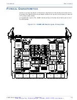
Page 56: ...AMP AV8 board have a thermal shunt that covers some of the components Figure 1 15 CHAMP AV8 Board Layout Primary Side Node A Processor U1 Node B Processor U2 SRIO Switch U84 Node A PCH U3 Node B PCH U4 PCIe Switch U128 Common Features FPGA Memory Mezzanine Connector Memory Mezzanine Connector Memory Mezzanine Connector Memory Mezzanine Connector P0 P1 P2 P3 P4 P5 P6 CPLD XMC J15 XMC J16 Ethernet X...

Page 57: ...S WRIGHT 1 36 PROPRIETARY 826448 VERSION 5 MARCH 2015 Figure 1 16 CHAMP AV8 Board Layout Secondary Side Node A NAND SSD Flash PABS Node B NAND SSD 1000 Base X Artisan Technology Group Quality Instrumentation Guaranteed 888 88 SOURCE www artisantg com ...

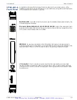
Page 58: ...ter that controls the green processor status LEDs seen opposite and two of the surface mount status LEDs on the PWB XMC Slot An opening is provided on the VPX6 462 A front panel to provide access to connectors that may be incorporated on an optional XMC module that may be installed on the basecard PWB If there is no XMC module mounted the opening is filled with a bezel J1 Connector The J1 connecto...

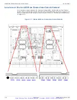
Page 59: ...he Processor Status LEDS the Fail LED and the Thermal Failure LED are all mounted on the top side of the board assembly as shown in Figure 1 17 below A description of LED behaviour can be found in Table 3 7 Summary of LED Behavior on page 3 15 Figure 1 17 Status LEDS on Conduction Cooled Variants Artisan Technology Group Quality Instrumentation Guaranteed 888 88 SOURCE www artisantg com ...

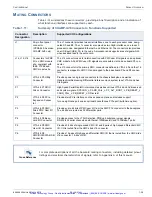
Page 60: ...s backplane as well as Geographical Addressing Differential reference clock system reset JTAG and Aux Clk signals P1 VITA 46 P1 SRIO Fabric Connector High Speed Serial RapidIO interconnect as well as various VITA 46 and AV8 reserved and system signals SYSCON_L CARD_FAIL_L CF_ALT_BOOT_L PB_RESET_L CARD_FAIL_L PB_RESET_L GDiscrete1 P2 VITA 46 P2 PCIe Expansion Connec tor Provides two PCIe interfaces...

Page 61: ... a variety of operating systems and development tools The following operating systems are supported on the CHAMP AV8 VxWorks 6 x Workbench 3 x from Wind River Part number DSW 462 000 VXW Fedora Linux Software Development Kit from Curtiss Wright part number DSW 462 001 LNX CONTINUUM IPC LIBRARY The Continuum Inter Processor Communications IPC Library available for the VxWorks OS platform only is a ...

Page 62: ... provides over 200 functions optimized for the SSE unit providing the foundation for most signal processing applications Continuum Vector provides the user with a choice of APIs with support for the Vector Signal Image Processing Library VSIPL Core Lite standard and the popular API established by Floating Point Systems Inc See the Continuum Vector data sheet for detailed information Artisan Techno...

Page 63: ...CHAMP AV8 VPX6 462 HARDWARE USER S MANUAL CURTISS WRIGHT 1 42 PROPRIETARY 826448 VERSION 5 MARCH 2015 Artisan Technology Group Quality Instrumentation Guaranteed 888 88 SOURCE www artisantg com ...

Page 64: ...s Requirements on page 2 2 Backplane Requirements on page 2 2 Detailed Power Requirements on page 2 3 BIOS Configuration Parameters on page 2 4 XMC Module Installation Requirements on page 2 4 XMC Site on page 2 4 Cable Requirements on page 2 6 Configuring Jumpers on page 2 7 Configuration Jumper Locations on page 2 8 Artisan Technology Group Quality Instrumentation Guaranteed 888 88 SOURCE www ar...

Page 65: ... air cooled chassis Conduction cooled Level 100 and Level 200 VPX6 462 C CHAMP AV8 cards are designed to be installed in a conduction cooled chassis BACKPLANE REQUIREMENTS The CHAMP AV8 boards are designed to be used with the VITA 65 backplanes with the following Slot and Module profiles Slot Profile SLT6 PAY 4F1Q2U2T 12 2 1 Module Profile MOD6 PAY 4F1Q2U2T 12 2 1 11 12 Warning To avoid personal i...

Page 66: ...te no on board circuitry uses these voltages When missing or below level backplane voltage other than 12V causes the board to be is held in a powered down state 12V is not gated to the XMC site thereby also powering down the XMC In order to ensure proper operation of the CHAMP AV8 board the remote voltage sense lines for the 12V and 3 3V power must be connected from the power supplies to the volta...

Page 67: ...XMC I O The CHAMP AV8 supports backplane user I O through the VPX connectors see CHAMP AV8 I O Mapping on page A 8 for details XMC SITE The VITA 42 standard and subsidiary specifications define the XMC mezzanine module format which adds high speed data interfaces and I O capability to the PMC standard Together these improvements allow for the next generation of mezzanine modules with improved thro...

Page 68: ...ard the thermal impact on the basecard should be assessed Caution When installing an XMC on the CHAMP AV8 careful characterization of the XMC performance should be done Technical Support may also be consulted Depending on the particular application and configuration various conditions can occur that could adversely affect and possibly extend oustide of the product specification the baseboard XMC o...

Page 69: ...62 FPL 000 CHAMP AV8 Standard Front Panel Cable Assembly Caution The CHAMP AV8 front panel cable is different than that used on the CHAMP AV6 even though the physical front panel connector is the same To use the CHAMP AV8 front panel the user must employ CBL 462 FPL 000 J1 J2 J3 J4 J5 SW1 RESET 36 2 Add heatshrink as Required to secure adapter Add 903075 000 assembly number label and associated re...

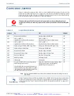
Page 70: ...OFT_JUMP1 1 registered and software defined jumper Off JB4 Enable writing to PROMs SPD GigE PCIe Write protect PROMs SPD GigE PCIe Off JB5 Enable writing to PABS Flash Write protect PABS Flash Off JB6 Write protect NVRAM Enable writing to NVRAM Off JB7 Write protect Primary Flash Enable writing to Primary Flash Off JB8 Boot from PABS site Boot from Primary Flash Off JB9 Watchdog disable Watchdog e...

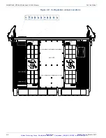
Page 71: ...IGHT 2 8 PROPRIETARY 826448 VERSION 5 MARCH 2015 Figure 2 2 Configuration Jumper Locations XMC SITE MMB2 U1 U2 MMB1 JB11 JB10 JB9 JB8 JB7 JB6 JB5 JB4 JB3 JB2 JB1 Artisan Technology Group Quality Instrumentation Guaranteed 888 88 SOURCE www artisantg com ...

Page 72: ...on page 3 4 Insert the Basecard in the Chassis on page 3 4 Connect a Terminal on page 3 5 Connect Ethernet Ports on page 3 6 CBL 462 FPL 000 Front Panel Cable Connections on page 3 8 Booting Entering the BIOS Setup Utility on page 3 11 Initiate the Power Up Sequence on page 3 12 Display the Initial Screen Message on page 3 13 Troubleshooting on page 3 14 Verify Insertion in Chassis on page 3 14 LE...

Page 73: ...r more detailed information describing the BIOS and the PBIT capabilities Warning This card uses components that are sensitive to electrostatic discharges It must be kept in its conductive package until the installation begins Remove the card from its protective package only at a grounded workstation while wearing an approved grounding wrist strap Avoid touching any metal contacts on the card stat...

Page 74: ...te cooling A front panel cable part number CBL 462 FPL 000 attached to a computer with a ter minal emulator program capable of operating at 115200 baud The front panel cable is used for air cooled variants only Standard Ethernet cables with RJ 45 connectors The Board Support Package CD ROM UNPACK AND CONFIGURE THE CARD Ensure that you complete the pre installation tasks described in Chapter 2 of t...

Page 75: ...een At power up the front panel red Fail LED should turn off see LED Diagnostics on page 3 14 If the red Fail LED fails to turn off turn the power off then check the seating of the card and verify that the chassis supplies the proper backplane power 12 V and 3 3 V DETAILED INSTALLATION PROCEDURE INSERT THE BASECARD IN THE CHASSIS Ensure that the chassis power is turned off before inserting the car...

Page 76: ...rd You can connect a terminal to the CHAMP AV8 in one of the following ways via the front panel connector see VPX6 462 A Front Panel on page 1 37 using front panel cable CBL 462 FPL 000 J2 for the air cooled version product only via the J2 connector for Node A or J3 connector for Node B using RTM6 462 000 to facil itate the connection available from the factory for both air cooled and conduc tion ...

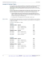
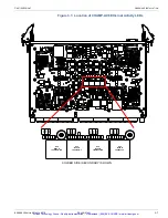
Page 77: ...e can be con nected to the 10 100 1000 ENET1 RJ 45 connector J9 connector for Node A and J10 connector for Node B on the RTM6 462 000 by wiring directly to the appropriate VPX P4 backplane connector pins Ethernet LEDs The CHAMP AV8 provides twelve LEDs on the bottom side of the PWB that provide link status and activity information for the Ethernet 1000 Base T and 1000 Base X ports See Figure 3 1 o...

Page 78: ...n of CHAMP AV8 Ethernet Activity LEDs SOLDER SIDE SECONDARY SHOWN U33 Node A 1000Base T U35 Node B 1000Base T DS1 DS2 DS3 DS17 DS16 DS15 DS22 DS23 DS24 DS4 DS5 DS6 U36 Node B 1000Base BX U34 Node A 1000Base BX Artisan Technology Group Quality Instrumentation Guaranteed 888 88 SOURCE www artisantg com ...

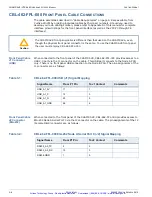
Page 79: ...ion to the Node B PCH The pin assignments of the J1 connector are as follows Front Panel Cable J2 Connector EIA 232 When connected to the front panel of the CHAMP AV8 CBL 462 FPL 000 provides access to EIA 232 Node A Serial Port 0 via the J2 connector on the cable The pin assignments of the J2 Female DB 9 connector are as follows Caution The CHAMP AV8 front panel cable is different than that used ...

Page 80: ...To J3 Contact Comments RS232_B0_TX 13 2 RS232_B0_RX 14 3 RS232 GND 1 5 Note The CHAMP AV8 serial ports do not provide access to the CTS and RTS signals Therefore software handshaking XON XOFF must be used Note The CHAMP AV8 EIA 232 serial channels are configured as DCE Data Communications Equipment The EIA 232 serial channels on personal computers and terminals are configured as DTE therefore a nu...

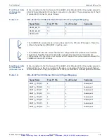
Page 81: ...et Port B J5 Signal Mapping Signal Name From P1 Pin To J5 Contact Comments ENET_B_TRD_P0 7 1 Twisted pair 1 ENET_B_TRD_N0 20 2 Twisted pair 1 ENET_B_TRD_P1 8 3 Twisted pair 2 ENET_B_TRD_N1 21 6 Twisted pair 2 ENET_B_TRD_P2 9 4 Twisted pair 3 ENET_B_TRD_N2 22 5 Twisted pair 3 ENET_B_TRD_P3 10 7 Twisted pair 4 ENET_B_TRD_N3 23 8 Twisted pair 4 Table 3 6 CBL 462 FPL 000 Reset Pushbutton SW1 Signal Ma...

Page 82: ...g system Once the resources are configured the PBIT application is executed if enabled PBIT validates operation of the hardware devices present on the board After completing initialization with a satisfactory result from PBIT the BIOS either transitions to an application program or interacts with the serial port accepting and processing maintenance commands Because the CHAMP AV8 does not contain a...

Page 83: ...eset controller turns on power supplies and asserts board reset signals according to preset timing Once the processors are powered each processor executes its BIOS contained in boot flash devices dedicated for each node During boot the user can elect to enter the BIOS setup utility by pressing the F2 key on a terminal connected via serial port to the CHAMP AV8 Each processor requires a separate se...

Page 84: ...ess the F2 key then you will see the following GRUB GRand Unified Bootloader loading message as follows Figure 3 3 GRUB Loading Message After a couple of seconds you will see Linux start loading ultimately concluding with the login prompt as shown below Linux AV8 2 6 39 3 45 SMP Fri Sep 7 10 44 41 EDT 2012 x86_64 x86_64 x86_64 GNU Linux Fedora release 10 AV8 login Artisan Technology Group Quality ...

Page 85: ...cessfully booted as described above Green Front Panel Processor Status LEDs At power on the eight front panel green Processor Status LEDs provide board status information After the CF FPGA has been successfully configured the green Processor Status LEDs will illuminate As the boot software initializes each processor node the software will turn the respective LED off Once the board has successfully...

Page 86: ...N Turned on by firmware OFF Defaults off and must be turned on by firmware when the pro cessor status is good Front Panel Air Cooled B0 DS25 1 Green Processor status indicator Node B core 0 Same as DS21 ON Turned on by firmware OFF Defaults off and must be turned on by firmware when the pro cessor status is good Front Panel Air Cooled B1 DS25 3 Green Processor status indicator Node B core 1 Same a...

Page 87: ...e as DS25 1 ON Turned on by firmware OFF Defaults off and must be turned on by firmware when the pro cessor status is good Top of PWB Conduction Cooled DS20 Green Processor status indicator Node B core 1 Same as DS25 3 ON Turned on by firmware OFF Defaults off and must be turned on by firmware when the pro cessor status is good Top of PWB Conduction Cooled DS19 Green Processor status indicator Nod...

Page 88: ...cates the 1000 Mbps link is estab lished and maintained N A Bottom of PWB DS16 Green Node A 1000Base T link status bit 1 ON Indicates the 1000Mbps link is estab lished and maintained Flashing Indicates the link is established and there is transmit or receive activity OFF Indicates the link is down Bottom of PWB DS17 Green Node A 1000Base T link status bit 2 ON Indicates the 1000Mbps link is estab ...

Page 89: ...r ation for 1000Base BX N A Bottom of PWB DS5 Green Node B 1000Base BX MDI Copper side interface link status bit 1 ON Indicates the link is established and there is no transmit and receive activity OFF Indicates the 1000Mbps link is down Bottom of PWB DS4 Green Node B 1000Base BX MDI Copper side interface link status bit 2 ON Indicates the 1000Mbps link is estab lished and maintained OFF Indicates...

Page 90: ...PWB DS8 Green 1000Base BX Reserved Reserved Bottom of PWB DS41 Red Configurator FPGA Load Status OFF Indicates FPGA loaded successfully ON Indicates FPGA failed to load successfully Bottom of PWB Air Cooled DS42 Red Thermal failure Indi cator Off Indicates the board is operating within its acceptable temperature range ON Indicates that an excessive temperature condition has been detected Top of PW...

Page 91: ...ot Mode turned off indicates successful boot and PBIT passed if PBIT enabled begins flashing indicates failure Recovery Boot Mode flashing Boot Inhibit Mode flashing SIGN ON MESSAGE GARBLED If the sign on message is garbled check that your terminal settings match 115200 8 N 1 115200 baud 8 data bits no parity 1 stop bit Also ensure that you are using a cable compatible with those listed in Cable R...

Page 92: ...ackplane J0 Utility Connector Pin Assignments on page A 16 CHAMP AV8 P1 SRIO Fabric Connector Pin Assignments on page A 17 Corresponding VPX Backplane J1 SRIO Fabric Connector Pin Assignments on page A 19 CHAMP AV8 P2 PCIe Expansion Connector Pin Assignments on page A 20 Corresponding VPX Backplane J2 PCIe Expansion Connector Pin Assignments on page A 22 CHAMP AV8 P3 XMC Site s PMC User I O Connec...

Page 93: ...ssignments on page A 35 J1 Front Panel Connector on page A 36 XMC Site s PMC J14 Connector on page A 39 XMC Site s PMC J14 User I O Connector on page A 39 XMC J15 and J16 Connectors on page A 42 XMC J15 Connector on page A 42 XMC J16 User I O Connector on page A 45 Rear Transition Module RTM on page A 52 Rear Transition Module Panel Mounted Connectors on page A 54 Rear Transition Module RTM Config...

Page 94: ... VITA 46 series standards define the details of VPX system connectors from the front plug in module to the backplane front side backplane rear side and Rear Transition Module RTM including mechanical dimensions part numbers and electrical pin definitions Figure A 1 below provides an illustration of how the VPX connectors are mated from a system point of view Figure A 1 VPX System Connectors Overvi...

Page 95: ...MP AV8 employs Tyco VPX RT2 connectors that incorporate a wafer style design that provides tightly controlled impedance low insertion loss and less than 3 crosstalk at signalling rates up to 6 25Gbaud By default the CHAMP AV8 is configured for 5Gbaud SRIO backplane interfaces The wafer converts a 7 row interface on the P CHAMP AV8 PWB side of the connector to a 9 row interface on the J backplane s...

Page 96: ...o Backplane Routings P0 J0 Connector Wafer Backplane PWB Backplane Row i h g f e d c b a hx gx cx dx gx cx Pwr 2 to f g h ix Pwr 1 to a b c dx bx fx hx ix Plug in Module PWB Plug in Row A B C D G E F ax ax bx ex fx ix dx Differential Plug in Module Wafer to Backplane Routings Even Wafers Connector Wafer Backplane PWB Backplane Row i h g f e d c b a GND hx gx GND GND cx dx GND GND GND dx GND GND gx...

Page 97: ...ers Table A 1 Wafer Usage CHAMP AV8 P0 Utility Connector Wafer Number Wafer Type 1 Power 2 Power 3 Power 4 Single Ended 5 Single Ended 6 Single Ended 7 Differential odd 8 Differential even Table A 2 Wafer Usage CHAMP AV8 P1 P6 Connectors Wafer Number Wafer Type 1 Differential odd 2 Differential even 3 Differential odd 4 Differential even 5 Differential odd 6 Differential even 7 Differential odd 8 ...

Page 98: ... Backplane P0 P6 Connector Orientation Connector Orientation i h g f e d c b a VITA46 P6 Wafer 1 to P6 Wafer 16 P5 Wafer 1 to P5 Wafer 16 P4 Wafer 1 to P4 Wafer 16 P3 Wafer 1 to P3 Wafer 16 P2 Wafer 1 to P2 Wafer 16 P1 Wafer 1 to P1 Wafer 16 P0 Wafer 1 to P0 Wafer 8 Artisan Technology Group Quality Instrumentation Guaranteed 888 88 SOURCE www artisantg com ...

Page 99: ...is mapped to the VITA 46 P5 and P6 connectors according to VITA 46 9 P5w3P6 X38s X8d X12d pattern See CHAMP AV8 P5 XMC User I O Connector Pin Assignments on page A 30 and CHAMP AV8 P6 XMC DIO SATA USB Connector Pin Assignments on page A 33 for details VITA 46 P0 Utility Connector The P0 connector on the CHAMP AV8 supports the following functions interfaces Power and Ground BP12V 3V3AUX 12AUX N12AU...

Page 100: ...user I O as per the VITA 46 9 P64s pattern No Connect NC Signals See Corresponding VPX Backplane J2 PCIe Expansion Connector Pin Assignments on page A 22 for additional details VITA 46 P4 Basecard I O Connector The P4 connector on the CHAMP AV8 supports the following functions interfaces CHAMP AV8 JTAG Selection Signals JTSEL_L JPROC 3 0 Reset Power Sequencer JTAG CPLD JTAG Chain Signals CHAMP AV8...

Page 101: ...A 33 for additional details USING THE CHAMP AV8 PINOUT CONFIGURATOR The backplane pinouts of the CHAMP AV8 vary according to the XMC modules installed on the basecard The Continuum Support Center website http csc cwcdefense com provides a Windows utility that generates the pinout configuration based on the modules installed This utility lets you choose from existing Curtiss Wright XMC modules or d...

Page 102: ... list for the single XMC slot on the CHAMP AV8 From the drop down list choose the module you have installed see Figure A 6 on page A 11 Cross Reference If your CHAMP AV8 has an XMC module installed that is not listed in the drop down list refer to Defining New XMC Modules on page A 13 Artisan Technology Group Quality Instrumentation Guaranteed 888 88 SOURCE www artisantg com ...

Page 103: ...AV8 click a Generate Pinout button The application displays the corresponding pinout table for your configuration as shown in the example in Figure A 7 below You may adjust the column widths of the table by dragging the column guides in the header row Figure A 7 Sample P5 Pinout Table Artisan Technology Group Quality Instrumentation Guaranteed 888 88 SOURCE www artisantg com ...

Page 104: ...New XMC button on the main window The Custom XMC window appears 2 Enter a name for the module 3 Enter the signal name for each pin in the text box corresponding to that pin 4 If you want to save the module for future use click the Save to File button 5 To use the new XMC module definition click the Add to XMC Lists button The new module is listed at the bottom of the drop down list in the main win...

Page 105: ...r Figure A 8 CHAMP AV8 P0 Utility Connector Table A 3 and Table A 4 on page A 15 describe the signals that are available on the P0 Utility connector on the CHAMP AV8 Cross Reference VPX is the name given to the family of VITA 46 standards available from http www VITA com For detailed information describing the mapping of the 7 row VPX board connectors to the 9 row VPX backplane connectors refer to...

Page 106: ...12V_AUX 12V Power 12V 5 Nominal Ripple 50 mV 1 A max GA4_L GA0_L GAP_L Geographical Address Inputs 0 4 and Parity Must pull up to 3 3V on board NVMRO Non Volatile Memory Read Only Active high signal that prevents any non volatile memory from being updated pulled up to 3 3VAUX on backplane can only be driven low by backplane Note this signal does not write enable the PABS Permanent Alternate Boot S...

Page 107: ... C Vs2_BP12V Vs2_BP12V Vs2_BP12V Vs2_BP12V 2 Vs1_BP12V Vs1_BP12V Vs1_BP12V Vs1_BP12V N C Vs2_BP12V Vs2_BP12V Vs2_BP12V Vs2_BP12V 3 Vs3_NC_BP_5V Vs3_NC_BP_5V Vs3_NC_BP_5V Vs3_NC_BP_5V N C Vs3_NC_BP_5V Vs3_NC_BP_5V Vs3_NC_BP_5V Vs3_NC_BP_5V 4 GND SM2_BP_I2C1_SCL SM3_BP_I2C1_DAT GND 12V_AUX GND SYSRST_L NVMRO GND 5 GND GAP_L GA4_L GND 3 3V_AUX GND SM0_BP_I2C0_SCL SM1_BP_I2C0_DAT GND 6 GND GA3_L GA2_L...

Page 108: ...gnal 1 BP_GDISCRETE1 GND PA_TX_N0 PA_TX_P0 GND PA_RX_N0 PA_RX_P0 2 GND PA_TX_N1 PA_TX_P1 GND PA_RX_N1 PA_RX_P1 GND 3 VBAT GND PA_TX_N2 PA_TX_P2 GND PA_RX_N2 PA_RX_P2 4 GND PA_TX_N3 PA_TX_P3 GND PA_RX_N3 PA_RX_P3 GND 5 SYS_CON_L GND PB_TX_N0 PB_TX_P0 GND PB_RX_N0 PB_RX_P0 6 GND PB_TX_N1 PB_TX_P1 GND PB_RX_N1 PB_RX_P1 GND 7 NC_RFU GND PB_TX_N2 PB_TX_P2 GND PB_RX_N2 PB_RX_P2 8 GND PB_TX_N3 PB_TX_P3 G...

Page 109: ... 24 26 28 30 CHAMP AV8 Signal Description BP_GDISCRETE1 Used for MBSC Sync Signal SYS_CON_L SYSCON_L VITA 46 0 signal that indicates which slot is the system controller Open collector driven by backplane pull up to 3 3V is implemented on board When driven low by the backplane the CHAMP AV8 will become the source of the SYSRST_L and REF_CLK_P N signals CF_ALT_BOOT_L Alternate Boot Enable Input Maps...

Page 110: ...B_TX_N0 PB_TX_P0 GND GND PB_RX_N0 PB_RX_P0 6 GND PB_TX_N1 PB_TX_P1 GND GND PB_RX_N1 PB_RX_P1 GND GND 7 NC_RFU GND GND PB_TX_N2 PB_TX_P2 GND GND PB_RX_N2 PB_RX_P2 8 GND PB_TX_N3 PB_TX_P3 GND GND PB_RX_N3 PB_RX_P3 GND GND 9 CF_ALT_BOOT_L GND GND PC_TX_N0 PC_TX_P0 GND GND PC_RX_N0 PC_RX_P0 10 GND PC_TX_N1 PC_TX_P1 GND GND PC_RX_N1 PC_RX_P1 GND GND 11 CARD_FAIL_L GND GND PC_TX_N2 PC_TX_P2 GND GND PC_R...

Page 111: ...e x4 PCIe ports on the CHAMP AV8 The pinout tables are presented in the order of the rows when looking from the backplane that is i h g f e d c b a Figure A 10 CHAMP AV8 VITA 46 P2 Connector See Table A 9 on page A 21 for connector pin assignments and Table A 10 on page A 21 for signal definitions Connector Orientation i h g f e d c b a VITA 46 P2 Wafer 1 to P2 Wafer 16 P0 P1 Artisan Technology Gr...

Page 112: ...D EP_12_PCIE_TX_N EP_12_PCIE_TX_P GND EP_12_PCIE_RX_N EP_12_PCIE_RX_P 14 GND EP_13_PCIE_TX_N EP_13_PCIE_TX_P GND EP_13_PCIE_RX_N EP_13_PCIE_RX_P GND 15 NC GND EP_14_PCIE_TX_N EP_14_PCIE_TX_P GND EP_14_PCIE_RX_N EP_14_PCIE_RX_P 16 GND EP_15_PCIE_TX_N EP_15_PCIE_TX_P GND EP_15_PCIE_RX_N EP_15_PCIE_RX_P GND Table A 10 P2 PCIe Expansion Plane Connector Signal Definitions CHAMP AV8 Signal Description E...

Page 113: ..._ TX_N EP_05_PCIE_ TX_P GND GND EP_05_PCIE_ RX_N EP_05_PCIE_ RX_P GND GND 7 NC GND GND EP_06_PCIE_ TX_N EP_06_PCIE_ TX_P GND GND EP_06_PCIE_ RX_N EP_06_PCIE_ RX_P 8 GND EP_07_PCIE_ TX_N EP_07_PCIE_ TX_P GND GND EP_07_PCIE_ RX_N EP_07_PCIE_ RX_P GND GND 9 NC GND GND EP_08_PCIE_ TX_N EP_08_PCIE_ TX_P GND GND EP_08_PCIE_ RX_N EP_08_PCIE_ RX_P 10 GND EP_09_PCIE_ TX_N EP_09_PCIE_ TX_P GND GND EP_09_PCI...

Page 114: ...site s J14 connector The pinout tables are presented in the order of the rows when looking from the backplane that is i h g f e d c b a Figure A 11 P3 XMC Site s PMC User I O Connector See Table A 12 on page A 24 for the connector pin assignments and Table A 12 on page A 24 for signal definitions VITA 46 Connector Orientation i h g f e d c b a P3 Wafer 1 to P3 Wafer 16 P0 P1 P4 P2 Artisan Technolo...

Page 115: ...5 PMC_27 GND PMC_26 PMC_28 8 GND PMC_29 PMC_31 GND PMC_30 PMC_32 GND 9 NC GND PMC_33 PMC_35 GND PMC_34 PMC_36 10 GND PMC_37 PMC_39 GND PMC_38 PMC_40 GND 11 NC GND PMC_41 PMC_43 GND PMC_42 PMC_44 12 GND PMC_45 PMC_47 GND PMC_46 PMC_48 GND 13 NC GND PMC_49 PMC_51 GND PMC_50 PMC_52 14 GND PMC_53 PMC_55 GND PMC_54 PMC_56 GND 15 NC GND PMC_57 PMC_59 GND PMC_58 PMC_60 16 GND PMC_61 PMC_63 GND PMC_62 PMC...

Page 116: ...PMC_13 PMC_15 GND GND PMC_14 PMC_16 GND GND 5 NC GND GND PMC_17 PMC_19 GND GND PMC_18 PMC_20 6 GND PMC_21 PMC_23 GND GND PMC_22 PMC_24 GND GND 7 NC GND GND PMC_25 PMC_27 GND GND PMC_26 PMC_28 8 GND PMC_29 PMC_31 GND GND PMC_30 PMC_32 GND GND 9 NC GND GND PMC_33 PMC_35 GND GND PMC_34 PMC_36 10 GND PMC_37 PMC_39 GND GND PMC_38 PMC_40 GND GND 11 NC GND GND PMC_41 PMC_43 GND GND PMC_42 PMC_44 12 GND P...

Page 117: ...secard I O of the CHAMP AV8 The pinout tables are presented in the order of the rows when looking from the backplane that is g f e d c b a Figure A 12 P4 Basecard I O Connector See Table A 15 on page A 27 for the connector pin assignments and Table A 16 on page A 27 for signal definitions P0 P1 P3 P2 P5 Connector Orientation i h g f e d c b a VITA46 P4 Wafer 1 to P4 Wafer 16 Artisan Technology Gro...

Page 118: ...TP_B_RX_N UTP_B_RX_P 12 GND UTP_A_TX_N UTP_A_TX_P GND UTP_A_RX_N UTP_A_RX_P GND 13 BP_PABS_B_S0 GND ETH_A_TRX1_N ETH_A_TRX1_P GND ETH_A_TRX0_N ETH_A_TRX0_P 14 GND ETH_A_TRX3_N ETH_A_TRX3_P GND ETH_A_TRX2_N ETH_A_TRX2_P GND 15 BP_PABS_B_SI GND ETH_B_TRX1_N ETH_B_TRX1_P GND ETH_B_TRX0_N ETH_B_TRX0_P 16 GND ETH_B_TRX3_N ETH_B_TRX3_P GND ETH_B_TRX2_N ETH_B_TRX2_P GND Table A 16 P4 Basecard I O Connect...

Page 119: ... _P N ETHA_TRX 3 _P N ETHB_TRX 0 _P N ETHB_TRX 1 _P N ETHB_TRX 2 _P N ETHB_TRX 3 _P N 1000Base T Nodes A and B GigE signals selected via build option between front panel J1 connector and backplane P4 connector GigE signals are not present on these pins when configured for front panel connection Mapped in accordance with VITA 65 specification UTPA_TX_P N UTPA_RX_P N UTPB_TX_P N UTPB_RX_P N 1000Base...

Page 120: ...MP_L_1 CF_SOFT_ JUMP_L_0 GND GND CF_WD_ DIS_L RS232_ A0_RX GND GND 7 BP_PABS_ A_SI GND GND RS422_RXA 2_N RS422_RXA 2_P GND GND RS422_TXA 2_N RS422_TXA 2_P 8 GND RS422_RXB2 _N RS422_RXB 2_P GND GND RS422_TXB2 _N RS422_TXB 2_P GND GND 9 BP_PABS_ B_CS0_L GND GND RS232_ A1_TX RS232_ A1_RX GND GND RS232_ A0_TX PMI_TRST_ L 10 GND RS232_ B0_TX RS232_ B0_RX GND GND RS232_ B1_TX RS232_ B1_RX GND GND 11 BP_...

Page 121: ... User I O of the CHAMP AV8 The pinout tables are presented in the order of the rows when looking from the backplane that is i h g f e d c b a Figure A 13 P5 XMC User I O Connector See Table A 18 on page A 31 for connector pin assignments and Table A 19 on page A 31 for signal definitions P1 P0 P4 P2 P3 P6 Connector Orientation i h g f e d c b a VITA46 P5 Wafer 1 to P5 Wafer 16 Artisan Technology G...

Page 122: ...GND XMC_A1 XMC_B1 GND XMC_D1 XMC_E1 14 GND XMC_A3 XMC_B3 GND XMC_D3 XMC_E3 GND 15 NC GND XMC_A11 XMC_B11 GND XMC_D11 XMC_E11 16 GND XMC_A13 XMC_B13 GND XMC_D13 XMC_E13 GND Table A 19 P5 XMC User I O Connector Signal Definitions CHAMP AV8 Signal Description XMC_C 19 01 XMC_F 19 01 XMC Single Ended User I O Mapping from XMC J16 connector 38 single ended signals These connection supports high speed s...

Page 123: ..._F02 XMC_F03 GND GND 5 NC GND GND XMC_C04 XMC_C05 GND GND XMC_F04 XMC_F05 6 GND XMC_C06 XMC_C07 GND GND XMC_F06 XMC_F07 GND GND 7 NC GND GND XMC_C08 XMC_C09 GND GND XMC_F08 XMC_F09 8 GND XMC_C10 XMC_C11 GND GND XMC_F10 XMC_F11 GND GND 9 NC GND GND XMC_C12 XMC_C13 GND GND XMC_F12 XMC_F13 10 GND XMC_C14 XMC_C15 GND GND XMC_F14 XMC_F15 GND GND 11 NC GND GND XMC_C16 XMC_C17 GND GND XMC_F16 XMC_F17 12 ...

Page 124: ...tor provides access to the XMC DIO SATA USB User I O of the CHAMP AV8 The pinout tables are presented in the order of the rows when looking from the backplane that is i h g f e d c b a Figure A 14 P6 XMC DIO PCIe Connector P0 P1 P3 P4 P5 P2 Connector Orientation i h g f e d c b a VITA46 P6 Wafer 1 to P6 Wafer 16 Artisan Technology Group Quality Instrumentation Guaranteed 888 88 SOURCE www artisant...

Page 125: ... SATA_B_TXN1 SATA_B_TXP1 GND SATA_B_RXN1 SATA_B_RXP1 10 GND NC NC GND NC NC GND 11 DIO5 GND NC NC GND NC NC 12 GND USB_A0_N USB_A0_P GND USB_B0_N USB_B0_P GND 13 DIO6 GND USB_A0_ POWER NC GND USB_B0_ POWER NC 14 GND NC NC GND NC NC GND 15 DIO7 GND DIO8 DIO9 GND DIO10 DIO11 16 GND DIO12 DIO13 GND DIO14 DIO15 GND Table A 22 P6 XMC DIO SATA USB Connector Signal Definitions CHAMP AV8 Signal Descriptio...

Page 126: ...A15 XMC_B15 GND GND XMC_D15 XMC_E15 GND GND 5 DIO2 GND GND XMC_A17 XMC_B17 GND GND XMC_D17 XMC_E17 6 GND XMC_A19 XMC_B19 GND GND XMC_D19 XMC_E19 GND GND 7 DIO3 GND GND NC NC GND GND NC NC 8 GND SATA_A_TXN1 SATA_A_TXP1 GND GND SATA_A_RXN1 SATA_A_RXP1 GND GND 9 DIO4 GND GND SATA_B_TXN1 SATA_B_TXP1 GND GND SATA_B_RXN1 SATA_B_RXP1 10 GND NC NC GND GND NC NC GND GND 11 DIO5 GND GND NC NC GND GND NC NC ...

Page 127: ...9 FP_ETH_B_P2 I O Front Panel Ethernet Port Node B IEEE 802 3 10 FP_ETH_B_P3 I O Front Panel Ethernet Port Node B IEEE 802 3 11 FP_USB_A_5V O USB Power USB 2 0 12 FP_USB_A_P I O USB Data USB 2 0 13 RS232_B0_TX O Front Panel Serial Port B TX EIA 232 14 RS232_B0_RX I Front Panel Serial Port B RX EIA 232 15 RS232_A0_RX I Front Panel Serial Port A RX EIA 232 16 FP_ETH_A_P3 I O Front Panel Ethernet Por...

Page 128: ...28 CHASSIS_GND CGND Chassis Ground CGND Note The CHAMP AV8 J1 front panel connector is designed for use with the front panel cable described in CBL 462 FPL 000 903075 000 on page 2 6 Table A 24 J1 Front Panel Connector Description Continued Artisan Technology Group Quality Instrumentation Guaranteed 888 88 SOURCE www artisantg com ...

Page 129: ...IGHT A 38 PROPRIETARY 826448 VERSION 5 MARCH 2015 Figure A 15 J1 Contact Numbering Arrangement Looking into the Front Panel J1 Pin 1 J1 Pin 26 J1 Pin 13 J1 Pin 14 Artisan Technology Group Quality Instrumentation Guaranteed 888 88 SOURCE www artisantg com ...

Page 130: ...egacy PMC user I O and is referenced as Pn4 Jn4 in the PMC specification IEEE 1386 1 2001 The table maps the J14 signals to the corresponding VITA 46 48 P3 connector pins The signals are differentially routed between the J14 connector and the P3 backplane connector in accordance with the P64s pattern defined in VITA 46 9d0 25 The adjacent signals in a given column on the P3 connector e g J14 01 an...

Page 131: ... F4 P3 E4 J14 15 I O J14 13 connection to P3 connector 14 P3 C4 P3 B4 J14 16 I O J14 14 connection to P3 connector 15 P3 E4 P3 F4 J14 13 I O J14 15 connection to P3 connector 16 P3 B4 P3 C4 J14 14 I O J14 16 connection to P3 connector 17 P3 E5 P3 D5 J14 19 I O J14 17 connection to P3 connector 18 P3 B5 P3 A5 J14 20 I O J14 18 connection to P3 connector 19 P3 D5 P3 E5 J14 17 I O J14 19 connection t...

Page 132: ...47 P3 E12 P3 F12 J14 45 I O J14 47 connection to P3 connector 48 P3 B12 P3 C12 J14 46 I O J14 48 connection to P3 connector 49 P3 E13 P3 D13 J14 51 I O J14 49 connection to P3 connector 50 P3 B13 P3 A13 J14 52 I O J14 50 connection to P3 connector 51 P3 D13 P3 E13 J14 49 I O J14 51 connection to P3 connector 52 P3 A13 P3 B13 J14 50 I O J14 52 connection to P3 connector 53 P3 F14 P3 E14 J14 55 I O ...

Page 133: ...and J16 as shown in Figure A 17 Figure A 17 Location of CHAMP AV8 XMC J15 and J16 Connectors XMC J15 CONNECTOR Table A 26 on page A 43 lists the pin assignments for the XMC J15 connector The J15 connector is the primary XMC connector as defined in V42 0 The XMC supports a single x8 x4 x2 or x1 PCI link in accordance with V42 3 U1 U2 U84 U3 U4 U128 XMC J15 Connector XMC J16 Connector Artisan Techno...

Page 134: ...C Connector Signal Definitions XMC Signal Description XMC_TX RXZ_P N 0 7 Differential Transmit Receive These signals are used by the XMC to transmit receive high speed protocol specific data to the carrier over the PCI Express interface B_CLK_PCH_SRC0_P N Differential reference clock for the PCI Express interface link This signal is generated by the carrier and transmitted to the mezzanine XMC_WAK...

Page 135: ...arrier to the XMC The CHAMP AV8 supplies 12V sequenced power on the VPWR power turn on will be delayed with respect to the backplane power 3V3 3 3 V Power pins The 3 3V power is regulated to within 3 3V 0 3V The power is sequenced with the 3V3 power supplied on the VPWR pins power turn on will be delayed with respect to the back plane power 3V3_AUX 3 3 V Auxiliary Power pin The 3 3V_AUX power is s...

Page 136: ...05 6 GND GND XMC_C06 GND GND XMC_F06 7 XMC_DP6_P XMC_DP6_N XMC_C07 XMC_DP7_P XMC_DP7_N XMC_F07 8 GND GND XMC_C08 GND GND XMC_F08 9 XMC_DP8_P XMC_DP8_N XMC_C09 XMC_DP9_P XMC_DP9_N XMC_F09 10 GND GND XMC_C10 GND GND XMC_F10 11 XMC_DP10_P XMC_DP10_N XMC_C11 XMC_DP11_P XMC_DP11_N XMC_F11 12 GND GND XMC_C12 GND GND XMC_F12 13 XMC_DP12_P XMC_DP12_N XMC_C13 XMC_DP13_P XMC_DP13_N XMC_F13 14 GND GND XMC_C1...

Page 137: ...on XMC module J16 A2 GND GND GND J16 A3 P5 F14 I O XMC_DP2_P connection to P5 connector Depends on XMC module J16 A4 GND GND GND J16 A5 P6 E1 I O XMC_DP4_P connection to P6 connector Depends on XMC module J16 A6 GND GND GND J16 A7 P6 F2 I O XMC_DP6_P connection to P6 connector Depends on XMC module J16 A8 GND GND GND J16 A9 P6 E3 I O XMC_DP8_P connection to P6 connector Depends on XMC module J16 A...

Page 138: ... XMC_DP2_N connection to P5 connector Depends on XMC module J16 B4 GND GND GND J16 B5 P6 D1 I O XMC_DP4_N connection to P6 connector Depends on XMC module J16 B6 GND GND GND J16 B7 P6 E2 I O XMC_DP6_N connection to P6 connector Depends on XMC module J16 B8 GND GND GND J16 B9 P6 D3 I O XMC_DP8_N connection to P6 connector Depends on XMC module J16 B10 GND GND GND J16 B11 P5 D15 I O XMC_DP10_N conne...

Page 139: ...onnector Depends on XMC module J16 C6 P5 F6 I O XMC_C06 connection to P5 connector Depends on XMC module J16 C7 P5 E6 I O XMC_C07 connection to P5 connector Depends on XMC module J16 C8 P5 E7 I O XMC_C08 connection to P5 connector Depends on XMC module J16 C9 P5 D7 I O XMC_C09 connection to P5 connector Depends on XMC module J16 C10 P5 F8 I O XMC_C10 connection to P5 connector Depends on XMC modul...

Page 140: ... XMC_DP3_P connection to P5 connector Depends on XMC module J16 D4 GND GND GND J16 D5 P6 B1 I O XMC_DP5_P connection to P6 connector Depends on XMC module J16 D6 GND GND GND J16 D7 P6 C2 I O XMC_DP7_P connection to P6 connector Depends on XMC module J16 D8 GND GND GND J16 D9 P6 B3 I O XMC_DP9_P connection to P6 connector Depends on XMC module J16 D10 GND GND GND J16 D11 P5 B15 I O XMC_DP11_P conne...

Page 141: ...ND J16 E3 P5 B14 I O XMC_DP3_N connection to P5 connector Depends on XMC module J16 E4 GND GND GND J16 E5 P6 A1 I O XMC_DP5_N connection to P6 connector Depends on XMC module J16 E6 GND GND GND J16 E7 P6 B2 I O XMC_DP7_N connection to P6 connector Depends on XMC module J16 E8 GND GND GND J16 E9 P6 A3 I O XMC_DP9_N connection to P6 connector Depends on XMC module J16 E10 GND GND GND J16 E11 P5 A15 ...

Page 142: ...XMC module J16 F6 P5 C6 I O XMC_F06 connection to P5 connector Depends on XMC module J16 F7 P5 B6 I O XMC_F07 connection to P5 connector Depends on XMC module J16 F8 P5 B7 I O XMC_F08 connection to P5 connector Depends on XMC module J16 F9 P5 A7 I O XMC_F09 connection to P5 connector Depends on XMC module J16 F10 P5 C8 I O XMC_F10 connection to P5 connector Depends on XMC module J16 F11 P5 B8 I O ...

Page 143: ...P AV8 An illustration of the various ports and the industry standard connectors provided by the RTM is shown below in Figure A 18 Figure A 18 CHAMP AV8 Rear Transition Module Views Additional interfaces and controls are made available on the RTM PWB as seen in Figure A 19 RTM Printed Wiring Board Component Side View on page A 53 Artisan Technology Group Quality Instrumentation Guaranteed 888 88 SO...

Page 144: ...Node B0 RS232 RESET SW7 P11 IPMI JTAG P15 SATA Tx Rx Eq P4 P5 DIO 8 15 DIO 0 7 P7 JB2 PMC I O SW8 SW9 SW10 SW11 SW12 SW16 SW14 SW3 SW4 SW5 SW6 SW15 SW2 SW13 SW17 SW18 GEO ADDR JTAG RS232 LOOP P1 P2 PABS B PABS A P12 P3 P6 JB7 JB8 IPMI I2C PMBUS JTAG WD_DIS ALT_ BOOT FLASH_ WR_DIS NVRAM_ WR_DIS PROM_ WR_EN NVMRO PABS_ WR_EN NAND_ WR_DIS JRPROC 0 3 PORT80_ EN_L JTSEL PMI_ JTSEL SOFT_ JMP 0 1 Configu...

Page 145: ... RTM The pin out for the two EIA 422 ports follows a Gigabit Ethernet pin out on an RJ 45 so that a 1000Base T Ethernet loopback cable can be used to loop each node s transmit data port to its respective receive data port The transmit signals are outputs from the RTM and the receive signals are inputs to the RTM The pin out is shown below in Table A 37 Table A 36 RTM ENET A J5 ENET B J6 Connector ...

Page 146: ...esting purposes Installing a jumper between transmit and receive loops transmits data back to the receive data line Figure A 20 Serial Port Loopback Control via RTM P3 Note Serial ports are labelled consecutively Ports 1 4 are EIA 232 and 5 6 are EIA 422 Table A 38 RTM EIA 232 COM Ports A D J2 J3 Connector Details Pin Number Signal Name Description 2 TX Data from processor UART 3 RX Data to proces...

Page 147: ...fore any EIA 232 cables should be removed prior to placing a port in loopback 2 Installing jumpers in the wrong orientation can potentially damage the board Be careful to install jumpers only as shown See Figure A 21 below Figure A 21 Proper Jumper Orientation for RTM P3 Jumpers NODE A0_TX NODE A1_TX NODE B0_TX NODE B1_TX NODE A0_RX NODE A1_RX NODE B0_RX NODE B1_RX X CORRECT INCORRECT Artisan Tech...

Page 148: ... for details about the NVMRO signal When in this state it is possible to enable writes to main NAND flash main boot flash NVRAM and FPGA PROM independent of the setting of the associated RTM switch This function ality is analogous to the VPX6 1957 Curtiss Wright Legacy Mode described in the VPX6 1957 Hardware User s Manual Cur tiss Wright document 830214 NVMRO signal is high unless driven low by a...

Page 149: ...ocument number 826450 for additional information describing the various boot modes and the operation of the SW0 and SW1 software jumpers Jumper settings may be viewed using the BSP refer to sysBoardInfoShow and sysJumperStateGet in the Software User s Manual CHAMP AV8 VxWorks BSP Driver Suite document number 826452 or in the Software User s Manual CHAMP AV8 Linux BSP Driver Suite document number 8...

Page 150: ...er factory use only P11 JTAG programming header factory use only P12 V46 0 Geographical Addressing Signals P13 Node A1 IDC 10 serial ports AT Everex standard P14 Node B1 IDC 10 serial ports AT Everex standard P15 SATA re drivers Transmit and Receive signal strength adjustment Table A 40 RTM Header Functions Continued Header Number Description Note Headers indicated as Factory use only are not inte...

Page 151: ..._35 35 36 PMC_36 PMC_37 37 38 PMC_38 PMC_39 39 40 PMC_40 PMC_41 41 42 PMC_42 PMC_43 43 44 PMC_44 PMC_45 45 46 PMC_46 PMC_47 47 48 PMC_48 PMC_49 49 50 PMC_50 PMC_51 51 52 PMC_52 PMC_53 53 54 PMC_54 PMC_55 55 56 PMC_56 PMC_57 57 58 PMC_58 PMC_59 59 60 PMC_60 PMC_61 61 62 PMC_62 PMC_63 63 64 PMC_64 Table A 41 RTM PMC I O JB2 Pin Assignments Continued PMC J14 Pin Odd Numbers JB2 Pin JB2 Pin PMC J14 Pi...

Page 152: ...A so that the CHAMP AV8 can determine which slot it is in These pins are also mapped to the P12 header on the RTM Table A 42 RTM Discrete I O P4 P5 Pin Assignments DIO 0 7 Signals P4 Pin P5 Pin DIO 8 15 Signals DIO0 2 2 DIO8 DIO1 4 4 DIO9 DIO2 6 6 DIO10 DIO3 8 8 DIO11 DIO4 10 10 DIO12 DIO5 12 12 DIO13 DIO6 14 14 DIO14 DIO7 16 16 DIO15 GND 1 3 5 7 9 11 15 1 3 5 7 9 11 15 GND Table A 43 RTM Geograph...

Page 153: ...n JB6 Pin Signal Name XMC_C01 1 2 XMC_F01 XMC_C02 3 4 XMC_F02 XMC_C03 5 6 XMC_F03 XMC_C04 7 8 XMC_F04 XMC_C05 9 10 XMC_F05 XMC_C06 11 12 XMC_F06 XMC_C07 13 14 XMC_F07 XMC_C08 15 16 XMC_F08 XMC_C09 17 18 XMC_F09 XMC_C10 19 20 XMC_F10 XMC_C11 21 22 XMC_F11 XMC_C12 23 24 XMC_F12 XMC_C13 25 26 XMC_F13 XMC_C14 27 28 XMC_F14 XMC_C15 29 30 XMC_F15 XMC_C16 31 32 XMC_F16 XMC_C17 33 34 XMC_F17 XMC_C18 35 36...

Page 154: ...1 12 XMC_DP12_N XMC_DP3_P 13 14 XMC_DP13_P XMC_DP3_N 15 16 XMC_DP13_N XMC_DP4_P 17 18 XMC_DP14_P XMC_DP4_N 19 20 XMC_DP14_N XMC_DP5_P 21 22 XMC_DP15_P XMC_DP5_N 23 24 XMC_DP15_N XMC_DP6_P 25 26 XMC_DP16_P XMC_DP6_N 27 28 XMC_DP16_N XMC_DP7_P 29 30 XMC_DP17_P XMC_DP7_N 31 32 XMC_DP17_N XMC_DP8_P 33 34 XMC_DP18_P XMC_DP8_N 35 36 XMC_DP18_N XMC_DP9_P 37 38 XMC_DP19_P XMC_DP9_N 39 40 XMC_DP19_N N C 41...

Page 155: ...CHAMP AV8 VPX6 462 HARDWARE USER S MANUAL CURTISS WRIGHT A 64 PROPRIETARY 826448 VERSION 5 MARCH 2015 Artisan Technology Group Quality Instrumentation Guaranteed 888 88 SOURCE www artisantg com ...

Page 156: ...OLATILITY IN THIS APPENDIX This appendix contains the Curtiss Wright Statement of Memory Volatility found in the following section CHAMP AV8 Statement of Volatility on page B 2 Artisan Technology Group Quality Instrumentation Guaranteed 888 88 SOURCE www artisantg com ...

Page 157: ...d power supply settings These settings are included in the table for the sake of completeness However in normal use a user cannot write data to these devices Table B 1 Memory Devices Available On The CHAMP AV8 Memory Type Size Volatility Function Accessible from CPU Write protection Note 1 Process to Clear SDRAM DDR3 4GB CPU Volatile Main SDRAM for the processors Yes None Remove Power NVRAM 256KB ...

Page 158: ...ial purpose hardware Note reprogramming would render card inoperable No None None PSU controller NVRAM ZL2008 Qty 12 1K Non volatile Controls CPU PSU set tings This can only be written with external special purpose hard ware No None None PSU controller NVRAM ZL2106 Qty 3 1K Non volatile Controls CPU PSU set tings This can only be written with external special purpose hard ware No None None Xilinx ...

Page 159: ... NVRMO signal must be logic High None EEPROM Dip Switch 24 bits Non volatile Board configuration Yes The memory is pro tected if jumper or wire wrap JB4 is NOT installed RTM SW12 must be Off Backplane NVRMO signal must be logic high None DDR3 SPD EEPROM 4 devices 4kbit Non volatile Contains DDR3 configu ration settings Yes The memory is pro tected if jumper or wire wrap JB4 is NOT installed RTM SW...

Page 160: ...information and procedures for hardware memory write protection It discusses the following topics NVRAM Write Protection on page C 2 BIOS SPI Flash Write Protection on page C 3 On Board SATA NAND Flash Write Protection on page C 4 Artisan Technology Group Quality Instrumentation Guaranteed 888 88 SOURCE www artisantg com ...

Page 161: ...e Write Protect jumper automatically protects the entire NVRAM not just the VPD reserved block This change is made even if the VPD is not moved from the NVRAM according to the procedure referenced below CHAMP AV8 early access boards with part number VPX6 462 A04B130 E were shipped with software storing VPD in the NVRAM Users are strongly encouraged to upgrade their BIOS and BSP to the latest versi...

Page 162: ...ther writes Eventually the process will time out and the BIOS boot continues Boot time increases by tens of seconds when the Boot Flash is fully write protected If the BIOS had not previously booted for instance when the BIOS Flash has been reprogrammed the BIOS will not complete the boot process with the Hardware Write Protect jumper in place Ensure the Hardware Write Protect jumper is not instal...

Page 163: ...part of its basic configuration caches its file system When cached it has been observed that a write protected SATA Flash may appear to delete a file Once the file system has been made coherent with the NAND Flash the deleted file will be seen to still be present Artisan Technology Group Quality Instrumentation Guaranteed 888 88 SOURCE www artisantg com ...

Page 164: ...JB3 pin assignments RTM A 61 E EIA 232 COM Ports A D J4 J7 RTM A 55 EIA 232 Serial Port Connectors RTM A 55 Electro Static Discharge ESD precautions 3 2 ENET 1 ENET 2 Connectors RTM A 54 Ethernet LEDs 3 6 F feature summary 1 3 front panel cable 3 8 G Geographical Addressing header pin assignments JB4 A 61 H hardware requirements 2 2 header connectors Rear Transition Module RTM A 58 I In This Chapt...

Page 165: ...A 58 Reset Pushbutton SW1 RTM A 58 RS422 Connector RTM A 54 RTM Printed Wiring Board layout A 53 RTM6 462 000 Rear Transition Module A 53 S serial communications connecting a terminal 3 5 serial port loopback control A 55 sign on message garbled 3 20 slot location 3 4 software 1 40 software development tools 1 41 software overview of available 1 40 specifications 1 31 SRIO Fabric connector P1 pin ...

Page 166: ...l service in house repair center WE BUY USED EQUIPMENT Sell your excess underutilized and idle used equipment We also offer credit for buy backs and trade ins www artisantg com WeBuyEquipment REMOTE INSPECTION Remotely inspect equipment before purchasing with our interactive website at www instraview com LOOKING FOR MORE INFORMATION Visit us on the web at www artisantg com for more information on ...

Reviews: