C
URTISS
-W
RIGHT
1
826448 V
ERSION
5 M
ARCH
2015
P
ROPRIETARY
A-45
XMC J16 U
SER
I/O C
ONNECTOR
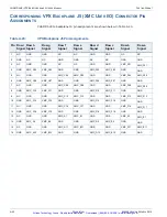
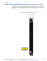
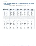
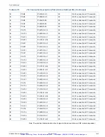
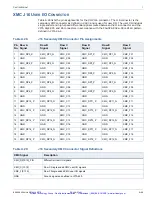
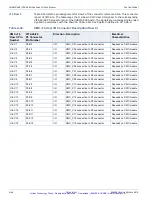
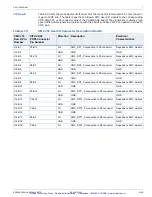
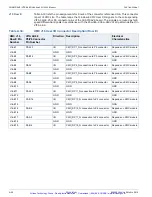
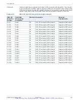
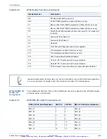
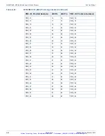
Table A.28 lists the pin assignments for the XMC J16 connector. The J16 connector is the
secondary XMC connector as defined in V42.0 and is used for user I/O. The user I/O includes
single ended and high speed differential signals routed between the J16 connector and the
VITA 46/48 P5 and P6 connectors in accordance with the P5w3P6–X38s+X8d+X12d pattern
defined in VITA 46.9.
Table A.28:
J16 Secondary XMC Connector Pin Assignments
Pin
No.
Row A
Signal
Row B
Signal
Row C
Signal
Row D
Signal
Row E
Signal
Row F
Signal
1
XMC_DP0_P
XMC_DP0_N
XMC_C01
XMC_DP1_P
XMC_DP1_N
XMC_F01
2
GND
GND
XMC_C02
GND
GND
XMC_F02
3
XMC_DP2_P
XMC_DP2_N
XMC_C03
XMC_DP3_P
XMC_DP3_N
XMC_F03
4
GND
GND
XMC_C04
GND
GND
XMC_F04
5
XMC_DP4_P
XMC_DP4_N
XMC_C05
XMC_DP5_P
XMC_DP5_N
XMC_F05
6
GND
GND
XMC_C06
GND
GND
XMC_F06
7
XMC_DP6_P
XMC_DP6_N
XMC_C07
XMC_DP7_P
XMC_DP7_N
XMC_F07
8
GND
GND
XMC_C08
GND
GND
XMC_F08
9
XMC_DP8_P
XMC_DP8_N
XMC_C09
XMC_DP9_P
XMC_DP9_N
XMC_F09
10
GND
GND
XMC_C10
GND
GND
XMC_F10
11
XMC_DP10_P
XMC_DP10_N
XMC_C11
XMC_DP11_P
XMC_DP11_N
XMC_F11
12
GND
GND
XMC_C12
GND
GND
XMC_F12
13
XMC_DP12_P
XMC_DP12_N
XMC_C13
XMC_DP13_P
XMC_DP13_N
XMC_F13
14
GND
GND
XMC_C14
GND
GND
XMC_F14
15
XMC_DP14_P
XMC_DP14_N
XMC_C15
XMC_DP15_P
XMC_DP15_N
XMC_F15
16
GND
GND
XMC_C16
GND
GND
XMC_F16
17
XMC_DP16_P
XMC_DP16_N
XMC_C17
XMC_DP17_P
XMC_DP17_N
XMC_F17
18
GND
GND
XMC_C18
GND
GND
XMC_F18
19
XMC_DP18_P
XMC_DP18_N
XMC_C19
XMC_DP19_P
XMC_DP19_N
XMC_F19
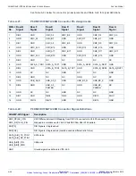
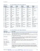
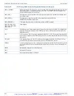
Table A.29:
J16 Secondary XMC Connector Signal Definitions
XMC Signal
Description
XMC_DP[0:19]_P/N
Differential User I/O signals
XMC_C[01:19]
Row C Single ended XMC user I/O signals
XMC_F[01:19]
Row F Single ended XMC user I/O signals
GND
Ground signals as defined in VITA 42.0.
Artisan Technology Group - Quality Instrumentation ... Guaranteed | (888) 88-SOURCE | www.artisantg.com


