24
AT40K Series Configuration
1009B–FPGA–03/02
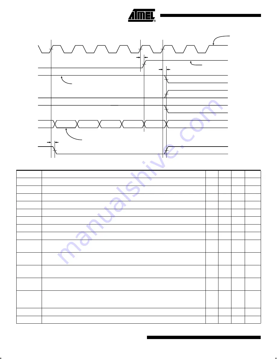
Figure 9.
Master Serial End of Configuration Download
t
CONH
DATA IN
x
x
LAST BIT OF POSTAMBLE
1
USER I/O
USER I/O
USER I/O
x
50K PULL-UP
(INTERNAL)
t
CFG
USER I/O
20K PULL-UP (INTERNAL)
x
10K PULL- UP
(INTERNAL)
1
CCLK
CON
INIT
LDC
HDC
USER I/O
ACTIVE ONLY IF CASCADE ENABLED
t
DCSOUT
CSOUT
Table 11.
Master Serial Configuration Timing Parameters @ 5V ± 10% Industrial/Commercial
Parameter
Description
Min
Typ
Max
Units
t
PPCCLK
Period of CCLK
0.6
1
1.6
µs
2 MHz option
300
500
800
ns
4 MHz option
150
250
400
ns
8 MHz option
75
125
200
ns
t
ICCLK
Delay from rising edge of INIT after reset to first rising edge of CCLK
1.8
3
4.8
ns
t
SCD
Setup time for Data with respect to rising edge of CCLK
6
10
16
ns
t
HCD
Hold time for Data with respect to rising edge of CCLK
0
0
0
ns
t
DCCLKH
Delay from falling edge of CON to first rising edge of CCLK to start recognition.
0.6
1
1.6
µs
t
SCCCLK
Setup time for CHECK with respect to rising edge of CCLK at the start of a configuration
download.
6
10
16
ns
t
DCI
Delay from rising edge of CCLK to activation of configuration interface pins at the start of
recognition.
6
10
16
ns
t
OE
Delay from rising edge of OE/RESET of AT17 Series configurator EEPROM to data valid
on Data Out of configurator. Data taken from the AT17 series datasheet.
150
ns
t
CE
Delay from falling edge of CON to Data valid from AT17 Series configurator EEPROM.
Data taken from the AT17 series datasheet.
45
ns
t
CONH
Delay from rising edge of CCLK to rising edge release of CON at the end of
configuration. Timing is measured with a 50pg load and a 2.7K pull-up resistor on CON.
Actual time will depend on system loading of CON.
130
ns
t
CFG
Delay from rising edge of CCLK to the release of dual-use pins to full user functionality.
6
10
16
ns
t
DCSOUT
Delay from rising edge of CCLK to CSOUT active at end of configuration.
6
10
16
ns


