


SERIES IP511 INDUSTRIAL I/O PACK ISOLATED QUAD EIA/TIA-422B COMMUNICATION MODULE
___________________________________________________________________________________________
- 5 -
Threaded metric M2 screws and spacers are supplied with the module
to provide additional stability for harsh environments (see Mechanical
Assembly Drawing 4501-434). The field and logic side connectors are
keyed to avoid incorrect assembly. P2 pin assignments are unique to
each IP model (see Table 2.1) and normally correspond to the pin
numbers of the field I/O interface connector on the carrier board (you
should verify this for your carrier board).
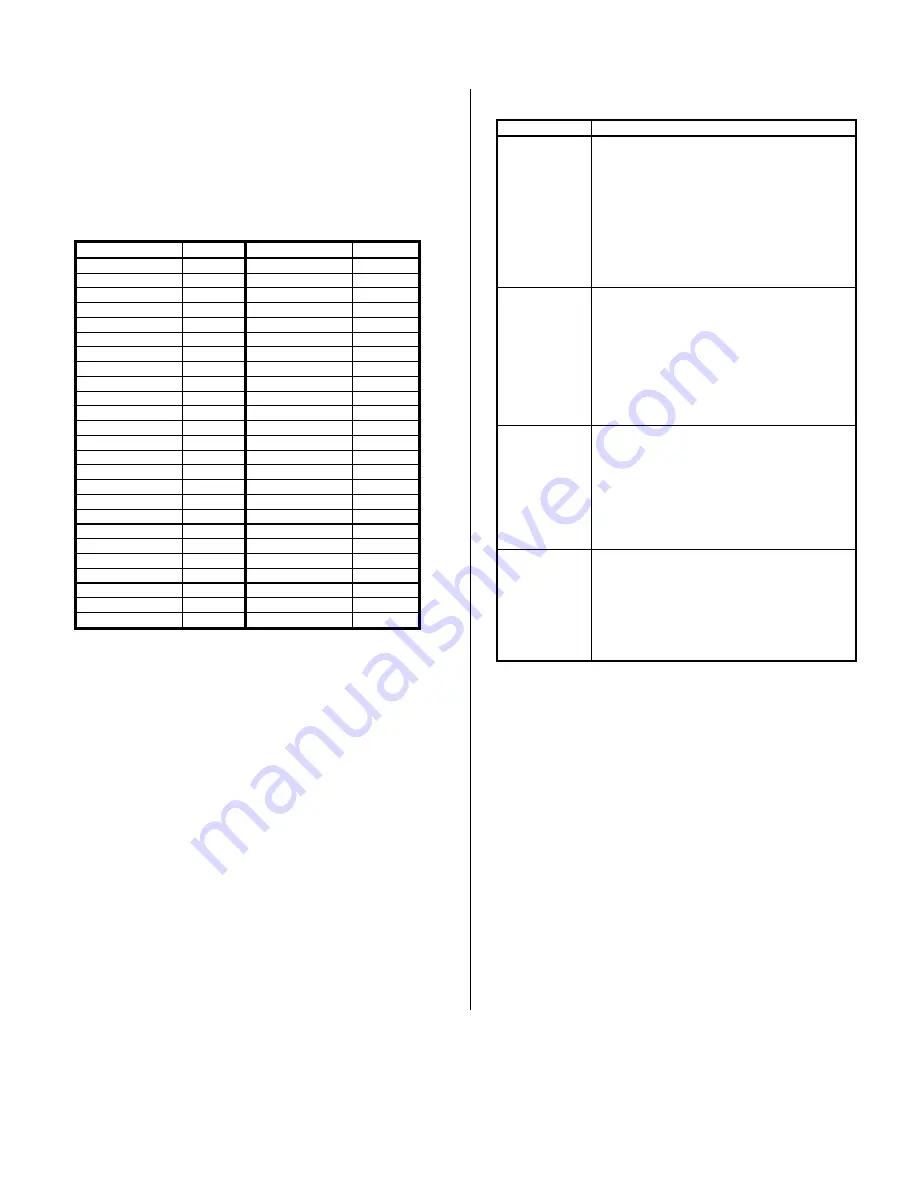
Table 2.1: IP511 Field I/O Pin Connections (P2)
Pin Description
Number
Pin Description
Number
COMMON A
1
COMMON C
26
+5V INPUT A
2
+5V INPUT C
27
TxDA+
3
TxDC+
28
+5V INPUT A
4
+5V INPUT C
29
TxDA-
5
TxDC-
30
+5V INPUT A
6
+5V INPUT C
31
RxDA-
7
RxDC-
32
+5V INPUT A
8
+5V INPUT C
33
RxDA+
9
RxDC+
34
COMMON B
10
COMMON D
35
+5V INPUT B
11
+5V INPUT D
36
TxDB+
12
TxDD+
37
+5V INPUT B
13
+5V INPUT D
38
TxDB-
14
TxDD-
39
+5V INPUT B
15
+5V INPUT D
40
RxDB-
16
RxDD-
41
+5V INPUT B
17
+5V INPUT D
42
RxDB+
18
RxDD+
43
Not Used
19
Not Used
44
Not Used
20
Not Used
45
Not Used
21
Not Used
46
Not Used
22
Not Used
47
Not Used
23
Not Used
48
Not Used
24
Not Used
49
Not Used
25
Not Used
50
An Asterisk (*) is used to indicate an active-low signal.
Refer to Table 2.1 and note that the pin-wire assignments are
arranged such that IDC D-SUB ribbon cable connectors can be
conveniently attached to provide serial port A (pins 1-9), serial port B
(pins 10-18), serial port C (pins 26-34), & serial port D (pins 35-43)
connectivity. Plus (+) and minus (-) following the signal name indicate
differential signal polarity. In Table 2.1, a suffix of “A”, “B”, “C”, or “D”
is appended to each pin label to denote its port association. A brief
description of each of the serial port signals at P2 is included below. A
complete functional description of the P2 pin functions is included in
Section 4.0 (Theory Of Operation). Be careful not to confuse the A-D
port designations of the IP module with the IP carrier board A-D slot
designations.
Note that none of the handshake lines of the UART are used by
this model and their corresponding UART input pins are tied high
(+5V). This includes, CTS (Clear-to-Send), RI (Ring Indicator), DCD
(Data Carrier Detect), and DSR (Data Set Ready). The RTS (Request-
to-Send) and DTR (Data Terminal Ready) output signal paths are not
connected. The port driver (transmit) and receivers are always enabled
on this model.
P2 Pin Signal Descriptions For Model IP511
SIGNAL
±±±±
DESCRIPTION
TxDA
±
TxDB
±
TxDC
±
TxDD
±
Transmit Data Line Differential Output Path. To
the communication network master, this line pair
is used as the transmit data path. To the
communication network slave, this line pair
comprises the receive data path. Because a
separate pair of lines are used for transit and
receive, full-duplex communication is implied.
During Loopback Mode, the TxD output of the
UART is internally connected to the RxD input
of the UART and disconnected from this data
path.
RxDA
±
RxDB
±
RxDC
±
RxDD
±
Receive Data Line Differential Input Path. To
the communication network master, this line pair
is the receive data path. To the communication
network slaves, this line comprises the transmit
data path. Because a separate pair of lines are
used for transmit and receive, full-duplex
communication is implied. During Loopback
Mode, the TxD output of the UART is internally
connected to the RxD input of the UART and
disconnected from this data path.
+5V INPUT A
+5V INPUT B
+5V INPUT C
+5V INPUT D
Is5V Port Power Input (four pin
connections per port). For isolated operation, an
external isolated power supply must be
connected here to power the port. If non-
isolated operation is acceptable, then the port
may be powered from the +5V logic supply of
the carrier by programming the port power and
ground jumpers accordingly (see Drawing 4501-
582).
COMMON A
COMMON B
COMMON C
COMMON D
Isolated Signal Common and +5V return. For
isolated operation, the external isolated power
supply common must be connected here to
complete power to the port. If non-isolated
operation is acceptable, then the port may be
powered from the logic common of the carrier by
programming the port power and ground
jumpers accordingly (see Drawing 4501-582).
Noise and Grounding Considerations
The serial ports of this module are isolated from the IP module’s
digital circuitry and from each other when external is5V power is
provided to the port. As long as separate isolated supplies are used,
the ports will also be isolated from each other. Otherwise, if the ports
share an isolated supply, they are isolated from the carrier, but not
isolated from each other. Optionally, the IP modules own +5V supply
and common may be jumpered to each port for non-isolated operation
(in this mode, the channels share a common signal ground and +5V
connection).
If isolated port power is not provided to the port connector and the
power jumpers are connecting the IP +5V and common to power the
port, then the signal ground connection at the communication ports are
common to each other and the IP interface ground, which is typically
common to safety (chassis) ground when mounted on a carrier board
and inserted in a backplane. As such, be careful not to attach signal
ground to safety ground in this mode via any device connected to these
ports, or a ground loop will be produced and this may adversely affect
operation.


