


SERIES IP511 INDUSTRIAL I/O PACK ISOLATED QUAD EIA/TIA-422B COMMUNICATION MODULE
___________________________________________________________________________________________
- 20 -
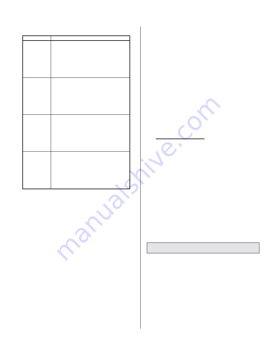
Port Signal Descriptions For Model IP511
SIGNAL
±±±±
DESCRIPTION
TxDA+, TxDA-
TxDB+, TxDB-
TxDC+, TxDC-
TxDD+, TxDD-
(DTE-to-DCE) Differential Port Driver Output
Positive & Negative. To the communication
network master, these line pairs comprise the
transmit data path. To the communication
network slaves, these lines are the receive data
path. During Loopback Mode, the TxD output of
the UART is internally connected to the RxD
input of the UART and disconnected from this
data path.
RxDA+, RxDA-
RxDB+, RxDB-
RxDC+,
RxDC-
RxDD+,
RxDD-
(DCE-to-DTE) Differential Port Receiver Input
Positive & Negative. To the communication
network master, these line pairs comprise the
receive data path. To the communication
network slaves, these lines are the transmit data
path. During Loopback Mode, the TxD output of
the UART is internally connected to the RxD
input of the UART and disconnected from this
data path.
+5V INPUT A
+5V INPUT B
+5V INPUT C
+5V INPUT D
Is5V Port Power Input (4 pin
connections per port). For isolated operation, an
external isolated power supply must be
connected here to power the port. If non-
isolated operation is acceptable, then the port
may be powered from the +5V logic supply
provided by the carrier by programming the
power and ground jumpers accordingly (see
Drawing 4501-582).
COMMON A
COMMON B
COMMON C
COMMON D
Individually Isolated Signal Common and +5V
returns. For isolated operation, the external
isolated power supply common must be
connected here to complete power to the port. If
non-isolated operation is acceptable, then the
port may be powered from the logic common
provided by the carrier by programming the
power and ground jumpers accordingly (see
Drawing 4501-582).
IP511 OPERATION
Connection to each serial port is provided through connector P2
(refer to Table 2.1). These pins are tied to the I/O pins of EIA/TIA-
422B line drivers and receivers (combined to form a transceiver). The
line receiver converts the EIA/TIA-422B received signal levels to the
TTL levels required by the UART (Universal Asynchronous
Receiver/Transmitter). The line drivers convert the UART TTL
transmitted levels to the EIA/TIA-422B voltages required at the
interface. The UART provides the necessary conversion from serial-to-
parallel (receive) and parallel-to-serial (transmit) for interfacing to the
data bus. Additionally, it provides data buffering and data formatting
capabilities. A programmable logic device is used to control the
interface between the UART, the IP bus, the line transceiver, and the
IDPROM.
Note that the field serial interface to the carrier board provided
through connector P2 (refer to Table 2.1) is considered isolated, only
when isolated external port power is provided to the port. Optionally, the
port may use P1 power by programming the power and common
jumpers appropriately. In this mode, the port is considered non-
isolated, and this means that the field signal return and logic common
have a direct electrical connection to each other. As such, care must
be taken to avoid ground loops (see Section 2 for connection
recommendations). Ignoring this effect may cause operation errors,
and with extreme abuse, possible circuit damage.
Refer to Drawing 4501-580 for example communication wiring and
grounding connections.
LOGIC/POWER INTERFACE
The logic interface to the carrier board is made through connector
P1 (refer to Table 2.2). Not all of the IP logic P1 pin functions are used.
P1 also pr5V to power the module (
±
12V is not used). For
model IP511, isolated port power is required separately.
A programmable logic device (PLD) installed on the IP Module
provides the control signals required to operate the board. The PLD
decodes the selected addresses in the I/O and ID spaces and produces
the chip selects, control signals, and signal timing required by the
UART communication registers. It also prioritizes the interrupt requests
coming from the serial ports in a shifting priority fashion, based on the
last interrupt serviced. Further, it generates the acknowledgement
signal required by the carrier board per the IP specification.
The ID PROM memory (read only) of the IP module provides the
identification for the individual module per the IP specification and is
implemented in the PLD. The ID PROM, configuration control
registers, and FIFO buffers are all accessed through an 8-bit data bus
interface to the carrier board.
5.0 SERVICE AND REPAIR
SERVICE AND REPAIR ASSISTANCE
Surface-Mounted Technology (SMT) boards are generally difficult
to repair. It is highly recommended that a non-functioning board be
returned to Acromag for repair. The board can be easily damaged
unless special SMT repair and service tools are used. Further,
Acromag has automated test equipment that thoroughly checks the
performance of each board. When a board is first produced and when
any repair is made, it is tested, placed in a burn-in room at elevated
temperature, and retested before shipment.
Please refer to Acromag's Service Policy Bulletin or contact
Acromag for complete details on how to obtain parts and repair.
PRELIMINARY SERVICE PROCEDURE
Before beginning repair, be sure that all of the procedures in
Section 2, Preparation For Use, have been followed. Also, refer to the
documentation of your carrier board to verify that it is correctly
configured. Replacement of the module with one that is known to work
correctly is a good technique to isolate a faulty module.
CAUTION: POWER MUST BE TURNED OFF BEFORE
REMOVING OR INSERTING BOARDS
Acromag’s Applications Engineers can provide further technical
assistance if required. When needed, complete repair services are also
available from Acromag.


