AXI Bridge for PCI Express v2.4
99
PG055 June 4, 2014
Appendix B:
Debugging
of
PCI Express Base Specification, rev. 2.1
states two rules that might be impacted by
FPGA Configuration Time:
• A component must enter the LTSSM Detect state within 20 ms of the end of the
Fundamental reset.
• A system must guarantee that all components intended to be software visible at boot
time are ready to receive Configuration Requests within 100 ms of the end of
Conventional Reset at the Root Complex.
These statements basically mean the FPGA must be configured within a certain finite time,
and not meeting these requirements could cause problems with link training and device
recognition.
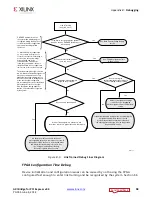
Configuration can be accomplished using an onboard PROM or dynamically using JTAG.
When using JTAG to configure the device, configuration typically occurs after the Chipset
has enumerated each peripheral. After configuring the FPGA, a soft reset is required to
restart enumeration and configuration of the device. A soft reset on a Windows based PC is
performed by going to
Start
>
Shut Down
and then selecting
Restart
.
To eliminate FPGA configuration as a root cause, you should perform a soft restart of the
system. Performing a soft reset on the system keeps power applied and forces
re-enumeration of the device. If the device links up and is recognized after a soft reset is
performed, then FPGA configuration is most likely the issue. Most typical systems use ATX
power supplies which provides some margin on this 100 ms window as the power supply is
normally valid before the 100 ms window starts.
Clock Debug
One reason to not deassert the
user_reset_out
signal is that the FPGA PLL (MMCM) and
Transceiver PLL have not locked to the incoming clock. To verify lock, monitor the
transceiver RXPLLLKDET output and the MMCM LOCK output. If the PLLs do not lock as
expected, it is necessary to ensure the incoming reference clock meets the requirements in
7 Series FPGAs GTX/GTH Transceivers User Guide
. The REFCLK signal should be routed
to the dedicated reference clock input pins on the serial transceiver, and the design should
instantiate the IBUFDS_GTE2 primitive in the design. See the
7 Series FPGAs GTX/GTH
Transceivers User Guide
for more information on PCB layout requirements, including
reference clock requirements.
Reference clock jitter can potentially close both the TX and RX eyes, depending on the
frequency content of the phase jitter. Therefore, maintain as clean a reference clock as
possible. Reduce crosstalk on REFCLK by isolating the clock signal from nearby high-speed
traces. Maintain a separation of at least 25 mils from the nearest aggressor signals. The PCI
Special Interest Group website provides other tools for ensuring the reference clocks are
compliant to the requirements of the
PCI Express Specification
:


