


106
WEB Interface
CP525 cMux User’s Manual Rev. 5.20.12 (3944)
ID: um_tsmux
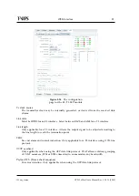
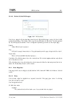
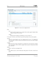
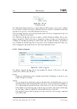
Figure 8.31
Clock regulator
Lock to external 1 PPS
Configures the internal clock to use the external 1 PPS input connector as reference.
The
Clock Regulator Status
field:
Regulator state
Idle
External reference signal is disabled.
Waiting
External Reference signal is enabled, but the internal clock has not obtained lock to
the reference
Fine tune
External Reference signal is enabled, and the internal clock has obtained lock to the
reference.
Current phase offset
Phase offset between the internal clock and 1 PPS clock reference given as a multiple of
3.704 ns (one period of 270 MHz)
Current freq. offset
Frequency offset between the internal clock and 1 PPS clock reference.
Current drift
Compensated frequency offset between external and internal reference.
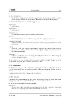
8.4.7.2 Alarms
These are the Clock regulator specific alarms. Clicking an alarm opens the field to configure
the alarm. Please see
for alarm configuration details.
Содержание CP525 cMux
Страница 1: ...CP525 cMux User s Manual Revision 5 20 12 3944 2012 12 17 Valid for SW version 5 20 12 and newer ...
Страница 2: ......
Страница 10: ......
Страница 12: ...12 CP525 cMux User s Manual Rev 5 20 12 3944 ID um_tsmux ...
Страница 18: ...18 CP525 cMux User s Manual Rev 5 20 12 3944 ID um_tsmux ...
Страница 24: ...24 CP525 cMux User s Manual Rev 5 20 12 3944 ID um_tsmux ...
Страница 66: ...66 CP525 cMux User s Manual Rev 5 20 12 3944 ID um_tsmux ...
Страница 238: ...238 CP525 cMux User s Manual Rev 5 20 12 3944 ID um_tsmux ...
Страница 248: ...248 CP525 cMux User s Manual Rev 5 20 12 3944 ID um_tsmux ...
Страница 276: ...276 CP525 cMux User s Manual Rev 5 20 12 3944 ID um_tsmux ...


