RFL 9785
RFL Electronics Inc.
June 18, 2009
18-4
(973) 334-3100
18.2.2
THEORY OF OPERATION
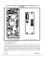
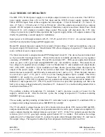
The RFL 9785, 50 Watt power supply is a multiple output, forward, dc to dc converter. The 106535-1
power supply operates from a 38 to 150 Vdc input, and the 106535-2 power supply operates from a
200 to 300 Vdc input. Each of these supplies has four outputs: +5 Vdc at 500 mAdc, +15 Vdc at 1.35
Adc, -15 Vdc at –1.00 Adc, and +12 Vdc at 250 mAdc. All of the outputs are connected to a common
ground. All DC outputs are constantly monitored. Should any output exceed lower limits Power Fault
Monitor (U9), will originate an under voltage signal. This signal will shut down the +12V relay
voltage to prevent any possible false operation due to power supply failure. All outputs contain or’ing
diodes for paralleling a second supply for redundancy.
Input power is fed through terminals A23-25, C23-25 and A30-32, C30-32. An external alarm and
interface board provides fusing and EMI suppression.
Diode CR1 protects the power supply from reversal of input voltage. Under such conditions, a fuse on
the power supply I/O board clears. Inrush limiter TH1 allows charging of capacitor C5 from a stiff dc
source without excessive input currents.
The forward converter is designed around PWM integrated circuit U1. The device has an internal clock
set by resistor R12 and capacitor C11. Power for the device is initially provided by a series regulator
consisting of MOSFET Q3, resistors R2 and R8, and diode CR5. With power applied and internal
clock set, pin 11 of U1 goes high causing MOSFET’s Q1, Q2, and Q5 to conduct. This causes the dc
bus voltage to be applied across windings 1 and 2 of transformer T1 and conduction of output diodes
CR7, CR9, CR11, and CR14. Upon conduction of these diodes, power flows from the input to the
output of the power supply. The dc bus current, which flows through MOSFET’s Q1 and Q2 is
detected across resistors R5 and R6 and is monitored at pins 3 and 4 of U1. When the peak increases
to a level set at pin 7 of U1, pin 11 of U1 is set low causing transistor Q4 to conduct. This drives
MOSFET’s Q1 and Q2 to an off state. Transformer T1 voltage reverses and diodes CR8, CR9
(opposite device), CR10, CR14 (opposite device) conduct and circulate current stored in inductor L3.
Inductor L3 and capacitors C19, C24, C26, and C34 form a low pass filter producing a dc that is the
half cycle average voltage produced by transformer T1. Inductor L3 is a multi-winding inductor that is
matched to transformer T1.
The auxiliary winding of transformer T1, terminals 5 and 6, provides a source of power for the
supply’s control circuit. After the first few cycles, the voltage at capacitor C17 increase rendering
MOSFET Q3 non-conductive.
The secondary auxiliary winding of transformer T1, terminals 3 and 4, capacitor C6, and diode CR2, is
a clamp to limit voltage transients across MOSFET’s Q1 and Q2.
The 5 Vdc output is unique because its level is monitored across diode CR6, resistors R42 and R43,
and potentiometer R44. The wiper arm of potentiometer R44 is fed to pin 6 of dual error amplifier U3
and is compared against an internal reference set at pin 7 of U3. If the 5Vdc output is greater than the
reference, pin 14 of U3 goes high causing optical isolator U2 to conduct. This reduces the voltage
applied to pin 5 of integrated circuit U1, reduces the peak current through transformer T1, and lowers
the output voltage. The negative feedback path is compensated with resistor R41 and C44.


