


RFL 9785
RFL Electronics Inc.
March 1, 2013
xiii
(973) 334-3100
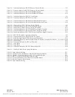
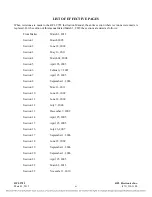
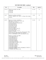
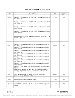
LIST OF TABLES
Table 2-1. Minimum permissible channel spacings and delays times,................................................................................. 2-5
Table 2-2. RFL 9785 modules, general information ............................................................................................................ 2-6
Table 4-1. Controls and indicators, RFL 9785 Front Panel ................................................................................................. 4-3
Table 4-2. Controls and indicator information for RFL 9785 system modules.................................................................... 4-4
Table 4-3. Input Attenuator Settings .................................................................................................................................. 4-14
Table 6-1. Controls and indicators, RFL 9785 AM Logic Module...................................................................................... 6-6
Table 6-2. Switch Settings, DIP Switch SW1 ...................................................................................................................... 6-7
Table 6-3. Switch Settings, DIP Switch SW1-6, -7, -8 ........................................................................................................ 6-7
Table 6-4. Switch Settings, DIP Switch SW2-1, -2, -3, -4................................................................................................... 6-7
Table 6-5. Switch Settings – Block Hold Timer, DIP Switch SW2-6, -7, -8....................................................................... 6-8
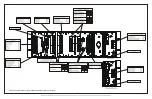
Table 9-1. Modules included in 9508 RF Chassis................................................................................................................. 9-2
Table 9-2. Input Voltage Ranges of Power Amplifier Power Supplies. ............................................................................... 9-7
Table 9-3. Motherboard Rear Panel Connector Assignments ............................................................................................. 9-17
Table 9-4. TB1 Terminal Assignments ............................................................................................................................... 9-18
Table 9-5. Module Placement In RF Chassis (50W System) .............................................................................................. 9-19
Table 9-6. 9508 RF Chassis Cables .................................................................................................................................... 9-21
Table 9-7. Analog Chassis Jumper Configurations And Other Settings ............................................................................. 9-24
Table 9-8. Function of jumpers, connectors and potentiometers on Power Amp. .............................................................. 9-26
Table 9-9. Function of DIP switches SW1 and SW2 on Power Amp Board ..................................................................... 9-27
Table 9-10. Tx Filter Setup Jumpers ................................................................................................................................... 9-28
Table 9-11. Setting Jumpers On Balance Board ................................................................................................................. 9-31
Table 9-12. Line Board Setup Jumpers and Switch Setting ................................................................................................ 9-33
Table 10-1. Controls and indicators, RFL 9785 Output Filter Modules ............................................................................ 10-4
Table 10-2. RFL 9785 Output Filter Modules, frequency ranges ...................................................................................... 10-6
Table 11-1. Controls and indicators, RFL9785 Receiver Downshifter Module ................................................................ 11-5
Table 11-2. Receive Frequency Select Switches................................................................................................................ 11-6