RFL 9785
RFL Electronics Inc.
December 7, 2009
13-3
(973) 334-3100
13.2.3
THEORY OF OPERATION
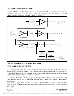
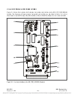
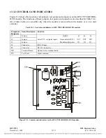
Refer to the schematic diagram in Figure 13-4 for the following discussion.
The RFL 9785 SOE/IRIG-B module consists of three major sections, the microcontroller section, the
IRIG-B section, and the reflected power section. The microcontroller section contains an 80C320
embedded microcontroller, an XILINX - XC9572 and associated support devices. The IRIG-B signal
section converts the incoming IRIG-B signal into an appropriate level signal that is fed to the
processor.
U3, U4, U5 and U6 form the heart of the processor circuit. U3 is an 80C320 8 bit embedded
microcontroller which monitors input status and decodes time information from the IRIG-B signal. U4
is a ROM that stores program code. U5 contains non-volatile RAM for storing SOE data and has a
built-in free running real time clock. U2 is a MAX691, which provides a reset pulse on power up and a
watchdog timer. U1 is an RS-232 Driver/Receiver. U6 is used to generate chip select signals for U11,
and SW1.
The IRIG-B circuits are used to convert the IRIG-B input signal to an appropriate level for the
80C320. It consists of a shunt regulator, a comparator, switches and an ICM7555.
SW1 is an eight position DIP switch which allows the user to set the mode of operation. For the RFL
9785 application, SW1-1, -2 and -3 should be in the ON position, and SW-5 should be in the ON
position. The processor reads this switch to set up the SOE/IRIG-B module. U11 is an input buffer for
16 input signals.
In the reflected power section DC input signals are fed into the board through J9, or the corresponding
edge connectors. The signals are filtered using a simple RC filter to remove noise picked up on the
input lines. The signals are then applied to the analog inputs of A/D converter U12. The inputs
represent the eight possible input signal functions, some of which are not used depending on the
chassis configuration. The multiplexed input signals at A13 and A19 each appear on two different
inputs of U12, one for each of the functions. Only one of these multiplexed functions is possible for
any particular chassis configuration. This is done to ease the processing of the signals in the
microprocessor.
U16 provides the -5v required by U12. Data is sent to the microprocessor using the standard data bus,
along with the normal read and write control signals. The other control signals for U12 are generated
by logic in the Actel processor interface chip U6. The A/D converter contains an internal reference.
The Actel circuit U11 is used to control the input digital signals to the microprocessor. Each of the
inputs (A21 - A28 and C21 - C28) passes through a debounce circuit which allows the output to
change only if the input has been in the same state for three consecutive sampling periods. The signals
are then multiplexed onto the DATAIN bus to the microprocessor. J6 is the JTAG input to J11.


