


CHAPTER 27 FLASH MEMORY
Page 827 of 920
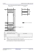
27.7.3
Procedure for accessing data flash memory
The data flash memory is initially stopped after a reset ends and cannot be accessed (read or programmed). To
access the memory, perform the following procedure:
<1> Write 1 to bit 0 (DFLEN) of the data flash control register (DFLCTL).
<2> Wait for the setup to finish for software timer, etc.
The time setup takes differs for each main clock mode.
<Setup time for each main clock mode>
• HS (High-speed main):
5
μ
s
• LS (Low-speed main):
720 ns
<3> After the wait, the data flash memory can be accessed.
Caution 1. Accessing the data flash memory is not possible during the setup time.
Caution 2. Transition to the STOP mode is not possible during the setup time. To enter the STOP mode
during the setup time, clear DFLEN to 0 and then execute the STOP instruction.
Caution 3. The high-speed on-chip oscillator should be kept operating during data flash rewrite. If it is
kept stopped, it should be operated (HIOSTOP = 0). The flash self-programming library should
be executed after 30
μ
s have elapsed.
Содержание RL78/G1H
Страница 941: ...R01UH0575EJ0120 RL78 G1H...


