Programming Sheets
B
-32
DSP56303 User’s Manual
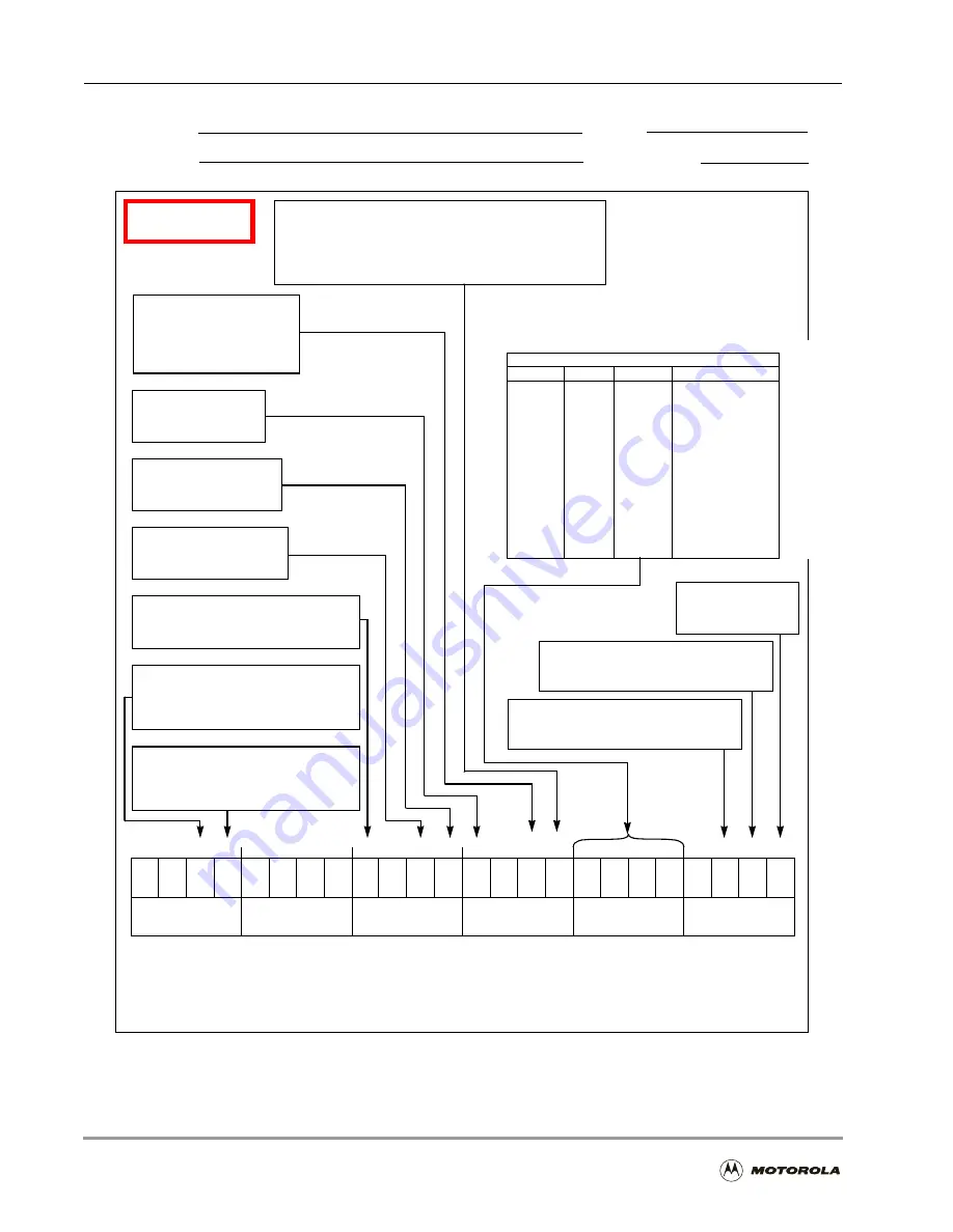
Figure B-21. Timer Control/Status Register (TCSR)
Application:
Date:
Programmer:
Sheet 2 of 3
15 14 13 12 11 10
9
8
7
6
5
4
3
2
1
0
TC3
TC1
TC0
TCIE TQIE
TE
19 18 17 16
23 22 21 20
TCF
TC2
PCE
DO
DI
DIR
TOF
TRM
INV
Timers
*
0
*
0
*
0
*
0
*
0
*
0
*
0
*
0
*
0
Timer Enable Bit 0
0 = Timer Disabled
1 = Timer Enabled
Timer Overflow Interrupt Enable Bit 1
0 = Overflow Interrupts Disabled
1 = Overflow Interrupts Enabled
Inverter Bit 8
0 = 0- to-1 transitions on TIO input increment the counter,
or high pulse width measured, or high pulse output on TIO
1 = 1-to-0 transitions on TIO input increment the counter,
or low pulse width measured, or low pulse output on TIO
Timer Compare Interrupt Enable Bit 2
0 = Compare Interrupts Disabled
1 = Compare Interrupts Enabled
Timer Control/Status Register
TCSR0:$FFFF8F Read/Write
TCSR1:$FFFF8B Read/Write
TCSR2:$FFFF87 Read/Write
Reset = $000000
*
= Reserved, Program as 0
Timer Reload Mode Bit 9
1 = Timer is reloaded when
selected condition occurs
0 = Timer operates as a free
running counter
Timer Overflow Flag Bit 20
0 = “1” has been written to TCSR(TOF),
or timer Overflow interrupt serviced
1 = Counter wraparound has occurred
Direction Bit 11
0 = TIO pin is input
1 = TIO pin is output
Data Output Bit 13
0 = Zero written to TIO pin
1 = One written to TIO pin
Data Input Bit 12
0 = Zero read on TIO pin
1 = One read on TIO pin
Timer Compare Flag Bit 21
0 = “1” has been written to TCSR(TCF),
or timer compare interrupt serviced
1 = Timer Compare has occurred
Prescaled Clock Enable Bit 15
0 = Clock source is CLK/2 or TIO
1 = Clock source is prescaler output
Timer Control Bits 4–7 (TC[3–0])
TC (3:0)
TIO
Clock
Mode
0000
0001
0010
0011
0100
0101
0110
0111
1000
1001
1010
1011
1100
1101
1110
1111
GPIO
Output
Output
Input
Input
Input
Input
Output
–
Output
Output
–
–
–
–
–
Internal
Internal
Internal
External
Internal
Internal
Internal
Internal
–
Internal
Internal
–
–
–
–
–
Timer
Timer Pulse
Timer Toggle
Event Counter
Input Width
Input Period
Capture
Pulse Width Modulation
Reserved
Watchdog Pulse
Watchdog Toggle
Reserved
Reserved
Reserved
Reserved
Reserved
Содержание DSP56303
Страница 1: ...DSP56303 User s Manual 24 Bit Digital Signal Processor DSP56303UM AD Revision 1 January 2001 ...
Страница 52: ...JTAG OnCE Interface 2 22 DSP56303 User s Manual ...
Страница 114: ...General Purpose Input Output GPIO 5 10 DSP56303 User s Manual ...
Страница 212: ...GPIO Signals and Registers 8 26 DSP56303 User s Manual ...
Страница 268: ...Interrupt Equates A 22 DSP56303 User s Manual ...
Страница 306: ...Programming Sheets B 38 DSP56303 User s Manual ...
Страница 320: ...Index 14 DSP56303 User s Manual ...


