


Overview
9
-2
DSP56303 User’s Manual
9.1.1
Triple Timer Module Block Diagram
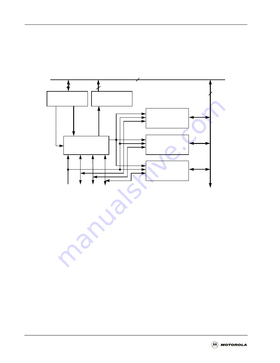
Figure 9-1 shows a block diagram of the triple timer module. This module includes a 24-bit
Timer Prescaler Load Register (TPLR), a 24-bit Timer Prescaler Count Register (TPCR), and
three timers. Each timer can use the prescaler clock as its clock source.
9.1.2
Individual Timer Block Diagram
Figure 9-2 shows the structure of an individual timer block. The DSP56303 treats each timer
as a memory-mapped peripheral with four registers occupying four 24-bit words in the X data
memory space. The three timers are identical in structure and function. Either standard polled
or interrupt programming techniques can be used to service the timers. A single, generic timer
is discussed in this chapter. Each timer includes the following:
n
24-bit counter
n
24-bit read/write Timer Control and Status Register (TCSR)
n
24-bit read-only Timer Count Register (TCR)
n
24-bit write-only Timer Load Register (TLR)
n
24-bit read/write Timer Compare Register (TCPR)
n
Logic for clock selection and interrupt/DMA trigger generation.
Figure 9-1. Triple Timer Module Block Diagram
Timer Prescaler
Count Register
GDB
24
24
TPLR
24
Timer 0
Timer 2
Timer 1
24-bit Counter
CLK/2
TIO0 TIO1 TIO2
TPCR
Timer Prescaler
Load Register
24
Содержание DSP56303
Страница 1: ...DSP56303 User s Manual 24 Bit Digital Signal Processor DSP56303UM AD Revision 1 January 2001 ...
Страница 52: ...JTAG OnCE Interface 2 22 DSP56303 User s Manual ...
Страница 114: ...General Purpose Input Output GPIO 5 10 DSP56303 User s Manual ...
Страница 212: ...GPIO Signals and Registers 8 26 DSP56303 User s Manual ...
Страница 268: ...Interrupt Equates A 22 DSP56303 User s Manual ...
Страница 306: ...Programming Sheets B 38 DSP56303 User s Manual ...
Страница 320: ...Index 14 DSP56303 User s Manual ...


