Programming Model
MOTOROLA
Synchronous Serial Interface (SSI)
30-19
30.3.7.1 I
2
S Mode Selection
The SCSR contains two bits, the I
2
S Mode Select (I2S MODE1 and I2S MODE0) bits, that determine the
mode of the SSI module. This section explains how the mode of the module affects the bits in the other SSI
registers. Table 30-8 summarizes the mode settings.
In normal mode operation, no register bits are forced to any particular state internally and the SSI can be
programmed to work in any operating condition.
When entering I
2
S modes (I
2
S master or I
2
S slave), several control bits are fixed in the hardware. Attempts
to write to these bits when in I
2
S master or I
2
S slave mode are ignored. These bits are described in
Table 30-9.
The user must configure the bit clock in the STCCR and the SRCCR.
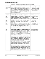
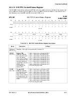
TFE
Bit 0
Transmit FIFO Empty
—Indicates that the data level in the
transmit FIFO reaches the Transmit FIFO Empty Water Mark.
The Water Mark is defined in the TFWM field of the SSI FIFO
Control/Status Register (SFCSR). The transmit FIFO must be
enabled or TFE is meaningless.
When TFE is set, data can be written to the transmit FIFO via the
STX register.
Note:
An interrupt is generated only when both the TFE and
TIE (of the STCR) are set and the transmit FIFO is enabled (the
TFEN bit in the STCR is set).
0 = Data level in the transmit
FIFO exceeds Water
Mark
1 = Data level in the transmit
FIFO below Watermark
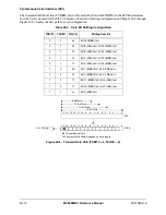
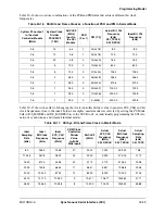
Table 30-8. I
2
S Mode Selection
I2S_MODE [1]
I2S_MODE [0]
Remark
0
0
Normal mode
0
1
I
2
S master mode
1
0
I
2
S slave mode
1
1
Normal mode
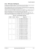
Table 30-9. I
2
S Master or I
2
S Slave Mode Settings
I
2
S Mode
Bit
Name
Register
Location
Forced
Value
Function
Master or save
SYN
SCSR [12]
1
Synchronous mode enabled
Master or save
NET
SCSR [11]
1
Network mode enabled
Master or save
TSHFD
STCR [4]
0
Transmission direction is MSB first
Master or save
RSHFD
SRCR [4]
0
Receive direction is MSB first
Master or save
TSCKP
STCR [3]
1
Falling edge of bit clock clocks data out
Table 30-7. SSI Control/Status Register Description (Continued)
Name
Description
Settings
Содержание DragonBall MC9328MX1
Страница 68: ...1 12 MC9328MX1 Reference Manual MOTOROLA Introduction ...
Страница 86: ...2 18 MC9328MX1 Reference Manual MOTOROLA Signal Descriptions and Pin Assignments ...
Страница 116: ...3 30 MC9328MX1 Reference Manual MOTOROLA Memory Map ...
Страница 126: ...4 10 MC9328MX1 Reference Manual MOTOROLA ARM920T Processor ...
Страница 160: ...8 8 MC9328MX1 Reference Manual MOTOROLA System Control ...
Страница 272: ...13 32 MC9328MX1 Reference Manual MOTOROLA DMA Controller ...
Страница 281: ...Programming Model MOTOROLA Watchdog Timer Module 14 9 ...
Страница 282: ...14 10 MC9328MX1 Reference Manual MOTOROLA Watchdog Timer Module ...
Страница 300: ...15 18 MC9328MX1 Reference Manual MOTOROLA Analog Signal Processor ASP ...
Страница 438: ...18 16 MC9328MX1 Reference Manual MOTOROLA Serial Peripheral Interface Modules SPI 1 and SPI 2 ...
Страница 478: ...19 40 MC9328MX1 Reference Manual MOTOROLA LCD Controller ...
Страница 542: ...20 64 MC9328MX1 Reference Manual MOTOROLA Multimedia Card Secure Digital Host Controller Module MMC SD ...
Страница 574: ...21 32 MC9328MX1 Reference Manual MOTOROLA Memory Stick Host Controller MSHC Module ...
Страница 598: ...23 16 MC9328MX1 Reference Manual MOTOROLA Real Time Clock RTC ...
Страница 670: ...24 72 MC9328MX1 Reference Manual MOTOROLA SDRAM Memory Controller ...
Страница 726: ...25 56 MC9328MX1 Reference Manual MOTOROLA SmartCard Interface Module SIM ...
Страница 736: ...26 10 MC9328MX1 Reference Manual MOTOROLA General Purpose Timers ...
Страница 854: ...29 18 MC9328MX1 Reference Manual MOTOROLA I2C Module ...
Страница 900: ...30 46 MC9328MX1 Reference Manual MOTOROLA Synchronous Serial Interface SSI ...
Страница 942: ...32 26 MC9328MX1 Reference Manual MOTOROLA GPIO Module and I O Multiplexer IOMUX ...


