


25-44
MC9328MX1 Reference Manual
MOTOROLA
SmartCard Interface Module (SIM)
25.7.4 Configuring the SIM General Purpose Counter
Table 25-29 provides the steps to configure the SIM general purpose counter for operation and the cross
references for identifying the specific section for additional reference.
25.7.5 Configuring the SIM Linear Redundancy Check Block
Table 25-30 provides the steps to configure the SIM linear redundancy check (LRC) block for operation
and the cross references for identifying the specific section for additional reference.
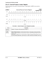
Table 25-29. Configuring the SIM General Purpose Counter
Step
Action
Reference
1.
Select desired clock source for the general purpose counter through
the GPCNT_CLK_SEL bits in the CNTL register.
Section 25.6.2, “Control Register,”
on page 25-23
2.
Program the counter comparator through the
GENERAL_PURPOSE_COUNTER bits in the GPCNT register to
select the desired count value at which the GPCNT interrupt flag is
set.
Section 25.6.16, “General Purpose
Counter Register,” on page 25-40
3.
Enable the selected clock source for the General Purpose Counter:
a. When the GP Counter is configured for the card clock, enable the
clock by setting the SIM_EN bit in the ENABLE register.
b. When the GP Counter is configured for the receive oversample
clock, enable this clock by setting the RCV_EN bit or the XMT_EN bit
in the ENABLE register.
c. When the GP Counter is configured for the transmit oversample
clock, enable this clock by setting the XMT_EN bit in the ENABLE
register.
Section 25.6.4, “Transmit/Receive
Enable Register,” on page 25-26
4.
Enable the general purpose counter interrupt through the GPCNTM
bit in the INT_MASK register.
Section 25.6.7, “Interrupt Mask
Register,” on page 25-31
Table 25-30. Configuring the SIM Linear Redundancy Check Block
Step
Action
Reference
1.
Enable the LRC block:
a. Use the LRCEN bit in the CNTL register.
b. Use the XMT_EN_LRC_CRC bit to enable the transmission of the
LRC Character after the last character in the Transmit FIFO is sent.
See the T = 1 programming model for more details.
Section 25.6.2, “Control Register,”
on page 25-23
Section 25.10.2.3 on page 25-54
Содержание DragonBall MC9328MX1
Страница 68: ...1 12 MC9328MX1 Reference Manual MOTOROLA Introduction ...
Страница 86: ...2 18 MC9328MX1 Reference Manual MOTOROLA Signal Descriptions and Pin Assignments ...
Страница 116: ...3 30 MC9328MX1 Reference Manual MOTOROLA Memory Map ...
Страница 126: ...4 10 MC9328MX1 Reference Manual MOTOROLA ARM920T Processor ...
Страница 160: ...8 8 MC9328MX1 Reference Manual MOTOROLA System Control ...
Страница 272: ...13 32 MC9328MX1 Reference Manual MOTOROLA DMA Controller ...
Страница 281: ...Programming Model MOTOROLA Watchdog Timer Module 14 9 ...
Страница 282: ...14 10 MC9328MX1 Reference Manual MOTOROLA Watchdog Timer Module ...
Страница 300: ...15 18 MC9328MX1 Reference Manual MOTOROLA Analog Signal Processor ASP ...
Страница 438: ...18 16 MC9328MX1 Reference Manual MOTOROLA Serial Peripheral Interface Modules SPI 1 and SPI 2 ...
Страница 478: ...19 40 MC9328MX1 Reference Manual MOTOROLA LCD Controller ...
Страница 542: ...20 64 MC9328MX1 Reference Manual MOTOROLA Multimedia Card Secure Digital Host Controller Module MMC SD ...
Страница 574: ...21 32 MC9328MX1 Reference Manual MOTOROLA Memory Stick Host Controller MSHC Module ...
Страница 598: ...23 16 MC9328MX1 Reference Manual MOTOROLA Real Time Clock RTC ...
Страница 670: ...24 72 MC9328MX1 Reference Manual MOTOROLA SDRAM Memory Controller ...
Страница 726: ...25 56 MC9328MX1 Reference Manual MOTOROLA SmartCard Interface Module SIM ...
Страница 736: ...26 10 MC9328MX1 Reference Manual MOTOROLA General Purpose Timers ...
Страница 854: ...29 18 MC9328MX1 Reference Manual MOTOROLA I2C Module ...
Страница 900: ...30 46 MC9328MX1 Reference Manual MOTOROLA Synchronous Serial Interface SSI ...
Страница 942: ...32 26 MC9328MX1 Reference Manual MOTOROLA GPIO Module and I O Multiplexer IOMUX ...