Programming Model
MOTOROLA
Analog Signal Processor (ASP)
15-11
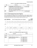
15.5.2 Pen A/D Sample Rate Control Register
The Pen A/D Sample Rate Control Register selects the sampling rate for touch pen input. Each application
may require different pen input sampling rates. The maximum A/D sampling rate is limited by the A/D
design and the input signal data setup time. The design is targeted to support up to a 200 Hz data rate for
each input signal. The user must set the data setup time and idle time for power saving.
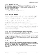
PADE
Bit 1
Pen A/D Enable
—Enables/Disables the Pen A/D
Controller. This bit must be set after all other control bits are
set. After this bit is set, A/D starts sampling. This bit must be
cleared by software when the touch penal is in idle state for
power saving
—
that is, waiting for a pen interrupt. When
this bit is clear, it flushes the Pen Sample FIFO.
0 = Pen A/D disabled
1 = Pen A/D enabled
BGE
Bit 0
Voltage Reference Enable
—Enables/Disables the voltage
reference circuit.
0 = Disable Voltage Ref
1 = Enable Voltage Ref
ASP_PSMPLRG
Pen A/D Sample Rate Control Register
Addr
0x00215014
BIT
31
30
29
28
27
26
25
24
23
22
21
20
19
18
17
16
TYPE
r
r
r
r
r
r
r
r
r
r
r
r
r
r
r
r
RESET
0
0
0
0
0
0
0
0
0
0
0
0
0
0
0
0
0X0000
BIT
15
14
13
12
11
10
9
8
7
6
5
4
3
2
1
0
DMCNT
BIT_SELECT
IDLECNT
DSCNT
TYPE
r
rw
rw
rw
rw
rw
rw
rw
rw
rw
rw
rw
rw
rw
rw
rw
RESET
0
0
0
0
0
0
0
0
0
0
0
0
0
0
0
0
0X0000
Table 15-8. Pen A/D Sample Rate Control Register Description
Name
Description
Settings
Reserved
Bits 31–15
Reserved—These bits are reserved and should read 0.
DMCNT
Bits 14–12
Decimation Ratio Count
—Controls the
decimation ratio of the second-stage FIR. Input
clock to this counter is fclk.
000 = Decimation ratio is 1
001 = Decimation ratio is 2
010 = Decimation ratio is 3
011 = Decimation ratio is 4
100 = Decimation ratio is 5
101 = Decimation ratio is 6
110 = Decimation ratio is 7
111 = Decimation ratio is 8
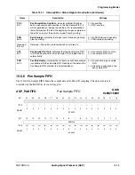
Table 15-7. Control Register Description (Continued)
Name
Description
Settings
Содержание DragonBall MC9328MX1
Страница 68: ...1 12 MC9328MX1 Reference Manual MOTOROLA Introduction ...
Страница 86: ...2 18 MC9328MX1 Reference Manual MOTOROLA Signal Descriptions and Pin Assignments ...
Страница 116: ...3 30 MC9328MX1 Reference Manual MOTOROLA Memory Map ...
Страница 126: ...4 10 MC9328MX1 Reference Manual MOTOROLA ARM920T Processor ...
Страница 160: ...8 8 MC9328MX1 Reference Manual MOTOROLA System Control ...
Страница 272: ...13 32 MC9328MX1 Reference Manual MOTOROLA DMA Controller ...
Страница 281: ...Programming Model MOTOROLA Watchdog Timer Module 14 9 ...
Страница 282: ...14 10 MC9328MX1 Reference Manual MOTOROLA Watchdog Timer Module ...
Страница 300: ...15 18 MC9328MX1 Reference Manual MOTOROLA Analog Signal Processor ASP ...
Страница 438: ...18 16 MC9328MX1 Reference Manual MOTOROLA Serial Peripheral Interface Modules SPI 1 and SPI 2 ...
Страница 478: ...19 40 MC9328MX1 Reference Manual MOTOROLA LCD Controller ...
Страница 542: ...20 64 MC9328MX1 Reference Manual MOTOROLA Multimedia Card Secure Digital Host Controller Module MMC SD ...
Страница 574: ...21 32 MC9328MX1 Reference Manual MOTOROLA Memory Stick Host Controller MSHC Module ...
Страница 598: ...23 16 MC9328MX1 Reference Manual MOTOROLA Real Time Clock RTC ...
Страница 670: ...24 72 MC9328MX1 Reference Manual MOTOROLA SDRAM Memory Controller ...
Страница 726: ...25 56 MC9328MX1 Reference Manual MOTOROLA SmartCard Interface Module SIM ...
Страница 736: ...26 10 MC9328MX1 Reference Manual MOTOROLA General Purpose Timers ...
Страница 854: ...29 18 MC9328MX1 Reference Manual MOTOROLA I2C Module ...
Страница 900: ...30 46 MC9328MX1 Reference Manual MOTOROLA Synchronous Serial Interface SSI ...
Страница 942: ...32 26 MC9328MX1 Reference Manual MOTOROLA GPIO Module and I O Multiplexer IOMUX ...


