Programming Model
MOTOROLA
External Interface Module (EIM)
11-15
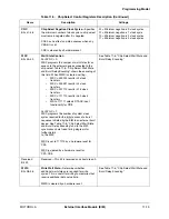
CNC
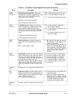
Bits 47–46
Chip Select Negation Clock Cycles
—Specifies
the minimum number of clock cycles a chip select
must remain negated after it is negated.
CNC has no effect on write accesses when any
CSA bit is set.
CNC is cleared by a hardware reset.
00 = Minimum negation is 0 clock cycles
01 = Minimum negation is 1 clock cycle
10 = Minimum negation is 2 clock cycles
11 = Minimum negation is 3 clock cycles
WSC
Bits 45–40
Wait State Control
—
For SYNC = 0:
WSC programs the number of wait-states for an
access to the external device connected to the
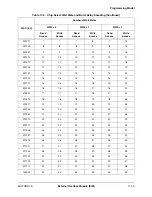
chip select. Table 11-6, "Chip Select Wait State
and Burst Delay Encoding" shows the encoding of
this field. When WWS is cleared, setting:
•
WSC = 000000 results in 2 clock
transfers
•
WSC = 000001 results in 2 clock
transfers
•
WSC = 001110 results in 15 clock
transfers
•
WSC = 111110 results in 63 clock
transfers
•
WSC=111111 selects DTACK input
functionality for CS5
For SYNC = 1:
WSC programs the number of system clock
cycles required for the initial access of a burst
sequence initiated by the EIM to an external burst
device. See Table 11-6, "Chip Select Wait State
and Burst Delay Encoding" and to the EIM
synchronous burst read timing diagrams for
further details.
to, the WSC
WSC is set to 111110 by a hardware reset for
CS0.
WSC is cleared by a hardware reset for
CS1–CS5.
See Table 11-6, "Chip Select Wait State and
Burst Delay Encoding"
Reserved
Bit 39
Reserved—This bit is reserved and should read 0.
WWS
Bits 38–36
Write Wait State
—Determines whether
additional wait-states are required for write
cycles. This is useful for writing to memories that
require additional data setup time.
WWS is cleared by a hardware reset.
See Table 11-6, "Chip Select Wait State and
Burst Delay Encoding"
Table 11-5. Chip Select Control Registers Description (Continued)
Name
Description
Settings
Содержание DragonBall MC9328MX1
Страница 68: ...1 12 MC9328MX1 Reference Manual MOTOROLA Introduction ...
Страница 86: ...2 18 MC9328MX1 Reference Manual MOTOROLA Signal Descriptions and Pin Assignments ...
Страница 116: ...3 30 MC9328MX1 Reference Manual MOTOROLA Memory Map ...
Страница 126: ...4 10 MC9328MX1 Reference Manual MOTOROLA ARM920T Processor ...
Страница 160: ...8 8 MC9328MX1 Reference Manual MOTOROLA System Control ...
Страница 272: ...13 32 MC9328MX1 Reference Manual MOTOROLA DMA Controller ...
Страница 281: ...Programming Model MOTOROLA Watchdog Timer Module 14 9 ...
Страница 282: ...14 10 MC9328MX1 Reference Manual MOTOROLA Watchdog Timer Module ...
Страница 300: ...15 18 MC9328MX1 Reference Manual MOTOROLA Analog Signal Processor ASP ...
Страница 438: ...18 16 MC9328MX1 Reference Manual MOTOROLA Serial Peripheral Interface Modules SPI 1 and SPI 2 ...
Страница 478: ...19 40 MC9328MX1 Reference Manual MOTOROLA LCD Controller ...
Страница 542: ...20 64 MC9328MX1 Reference Manual MOTOROLA Multimedia Card Secure Digital Host Controller Module MMC SD ...
Страница 574: ...21 32 MC9328MX1 Reference Manual MOTOROLA Memory Stick Host Controller MSHC Module ...
Страница 598: ...23 16 MC9328MX1 Reference Manual MOTOROLA Real Time Clock RTC ...
Страница 670: ...24 72 MC9328MX1 Reference Manual MOTOROLA SDRAM Memory Controller ...
Страница 726: ...25 56 MC9328MX1 Reference Manual MOTOROLA SmartCard Interface Module SIM ...
Страница 736: ...26 10 MC9328MX1 Reference Manual MOTOROLA General Purpose Timers ...
Страница 854: ...29 18 MC9328MX1 Reference Manual MOTOROLA I2C Module ...
Страница 900: ...30 46 MC9328MX1 Reference Manual MOTOROLA Synchronous Serial Interface SSI ...
Страница 942: ...32 26 MC9328MX1 Reference Manual MOTOROLA GPIO Module and I O Multiplexer IOMUX ...


