Programming Model
MOTOROLA
Universal Asynchronous Receiver/Transmitters (UART) Modules
27-35
27.7.6 UART Control Register 4
The UART Control Register 4s control the operation of some of the UART interrupts.
UCR4_1
UCR4_2
UART1 Control Register 4
UART2 Control Register 4
Addr
0x0020608C
0x0020708C
BIT
31
30
29
28
27
26
25
24
23
22
21
20
19
18
17
16
TYPE
r
r
r
r
r
r
r
r
r
r
r
r
r
r
r
r
RESET
0
0
0
0
0
0
0
0
0
0
0
0
0
0
0
0
0x0000
BIT
15
14
13
12
11
10
9
8
7
6
5
4
3
2
1
0
CTSTL
INVR
ENIRI
WKEN
REF16
IRSC
TCEN
BKEN
OREN
DREN
TYPE
rw
rw
rw
rw
rw
rw
rw
rw
rw
rw
rw
r
rw
rw
rw
rw
RESET
1
0
0
0
0
0
0
0
0
1
0
0
0
0
0
0
0x8040
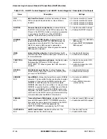
Table 27-18. UART1 Control Register 4 and UART2 Control Register 4 Description
Name
Description
Settings
Reserved
Bits 31–16
Reserved—These bits are reserved and should read 0.
CTSTL
Bits 15–10
CTS Trigger Level
—Controls the threshold at which the
CTS pin is deasserted by the RxFIFO. After the trigger
level is reached and the CTS pin is deasserted, the
RxFIFO continues to receive data until it is full. The CTSTL
bits are encoded as shown in the Settings column.
000000 = 0 characters received
000001 = 1 characters in the RxFIFO
...
100000 = 32 characters in the RxFIFO
(maximum)
All Other Settings Reserved
INVR
Bit 9
Inverted Infrared Reception
—Determines the logic level
for the detection. When cleared, the infrared logic block
expects an active low or negative IR 3/16 pulse for 0s and
1s are expected for 1s. When INVR is set (INVR
=
1), the
infrared logic block expects an active high or positive IR
3/16 pulse for 0s and 0s are expected for 1s.
0 = Active low detection
1 = Active high detection
ENIRI
Bit 8
Serial Infrared Interrupt Enable
—Enables/Disables the
serial infrared interrupt.
0 = Serial infrared Interrupt disabled
1 = Serial infrared Interrupt enabled
WKEN
Bit 7
WAKE Interrupt Enable
—Enables/Disables the WAKE bit
to generate an interrupt. The WAKE bit is set at the
detection of a start bit by the receiver.
0 = Disable the WAKE interrupt
1 = Enable the WAKE interrupt
REF16
Bit 6
Reference Frequency 16 MHz
—Indicates to the hardware
that a reference clock of 16 MHz is used. The reference
clock is derived from input clock IPG_CLK via the
programmable divider.
0 = 16 MHz reference clock not used
1 = 16 MHz reference clock is used
Содержание DragonBall MC9328MX1
Страница 68: ...1 12 MC9328MX1 Reference Manual MOTOROLA Introduction ...
Страница 86: ...2 18 MC9328MX1 Reference Manual MOTOROLA Signal Descriptions and Pin Assignments ...
Страница 116: ...3 30 MC9328MX1 Reference Manual MOTOROLA Memory Map ...
Страница 126: ...4 10 MC9328MX1 Reference Manual MOTOROLA ARM920T Processor ...
Страница 160: ...8 8 MC9328MX1 Reference Manual MOTOROLA System Control ...
Страница 272: ...13 32 MC9328MX1 Reference Manual MOTOROLA DMA Controller ...
Страница 281: ...Programming Model MOTOROLA Watchdog Timer Module 14 9 ...
Страница 282: ...14 10 MC9328MX1 Reference Manual MOTOROLA Watchdog Timer Module ...
Страница 300: ...15 18 MC9328MX1 Reference Manual MOTOROLA Analog Signal Processor ASP ...
Страница 438: ...18 16 MC9328MX1 Reference Manual MOTOROLA Serial Peripheral Interface Modules SPI 1 and SPI 2 ...
Страница 478: ...19 40 MC9328MX1 Reference Manual MOTOROLA LCD Controller ...
Страница 542: ...20 64 MC9328MX1 Reference Manual MOTOROLA Multimedia Card Secure Digital Host Controller Module MMC SD ...
Страница 574: ...21 32 MC9328MX1 Reference Manual MOTOROLA Memory Stick Host Controller MSHC Module ...
Страница 598: ...23 16 MC9328MX1 Reference Manual MOTOROLA Real Time Clock RTC ...
Страница 670: ...24 72 MC9328MX1 Reference Manual MOTOROLA SDRAM Memory Controller ...
Страница 726: ...25 56 MC9328MX1 Reference Manual MOTOROLA SmartCard Interface Module SIM ...
Страница 736: ...26 10 MC9328MX1 Reference Manual MOTOROLA General Purpose Timers ...
Страница 854: ...29 18 MC9328MX1 Reference Manual MOTOROLA I2C Module ...
Страница 900: ...30 46 MC9328MX1 Reference Manual MOTOROLA Synchronous Serial Interface SSI ...
Страница 942: ...32 26 MC9328MX1 Reference Manual MOTOROLA GPIO Module and I O Multiplexer IOMUX ...


