Programming Model
MOTOROLA
DMA Controller
13-21
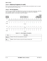
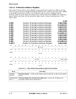
13.4.3.3 Channel Count Registers
Each of the channel count registers (CNTRx) contain the number of bytes of data to be transferred. There
is an internal counter that counts up (number of bytes—4 for word, 2 for halfword and 1 for byte) for every
DMA transfer. The internal counter is compared with the register after every transfer. When the counter
value matches with the register value, the channel is disabled until the CEN bit is cleared and set again, or
the RPT bit in the corresponding channel control register is set to
1
. The internal counter is reset to
0
when
the channel is enabled again.
The length of the last DMA burst can be shorter than the regular burst length specified in the burst length
register. However, when data is transferred out from an I/O FIFO and the last burst is less than BL, the I/O
device must generate a DMA request for the last transfer. When data is transferred to an I/O FIFO and the
last burst is less than BL, only the remaining number of data is transferred.
When the source mode is set to end-of-burst enable FIFO, this register becomes a read only register and the
value of the register is the number of bytes being transferred.
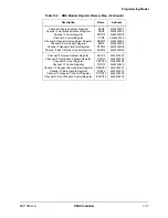
CNTR0
CNTR1
CNTR2
CNTR3
CNTR4
CNTR5
CNTR6
CNTR7
CNTR8
CNTR9
CNTR10
Channel 0 Count Register
Channel 1 Count Register
Channel 2 Count Register
Channel 3 Count Register
Channel 4 Count Register
Channel 5 Count Register
Channel 6 Count Register
Channel 7 Count Register
Channel 8 Count Register
Channel 9 Count Register
Channel 10 Count Register
Addr
0x00209088
0x002090C8
0x00209108
0x00209148
0x00209188
0x002091C8
0x00209208
0x00209248
0x00209288
0x002092C8
0x00209308
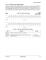
BIT
31
30
29
28
27
26
25
24
23
22
21
20
19
18
17
16
CNT
TYPE
r
r
r
r
r
r
r
r
rw
rw
rw
rw
rw
rw
rw
rw
RESET
0
0
0
0
0
0
0
0
0
0
0
0
0
0
0
0
0x0000
BIT
15
14
13
12
11
10
9
8
7
6
5
4
3
2
1
0
CNT
TYPE
rw
rw
rw
rw
rw
rw
rw
rw
rw
rw
rw
rw
rw
rw
rw
rw
RESET
0
0
0
0
0
0
0
0
0
0
0
0
0
0
0
0
0x0000
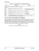
Table 13-16. Channel Count Registers Description
Name
Description
Reserved
Bits 31–24
Reserved—These bits are reserved and should read 0.
Содержание DragonBall MC9328MX1
Страница 68: ...1 12 MC9328MX1 Reference Manual MOTOROLA Introduction ...
Страница 86: ...2 18 MC9328MX1 Reference Manual MOTOROLA Signal Descriptions and Pin Assignments ...
Страница 116: ...3 30 MC9328MX1 Reference Manual MOTOROLA Memory Map ...
Страница 126: ...4 10 MC9328MX1 Reference Manual MOTOROLA ARM920T Processor ...
Страница 160: ...8 8 MC9328MX1 Reference Manual MOTOROLA System Control ...
Страница 272: ...13 32 MC9328MX1 Reference Manual MOTOROLA DMA Controller ...
Страница 281: ...Programming Model MOTOROLA Watchdog Timer Module 14 9 ...
Страница 282: ...14 10 MC9328MX1 Reference Manual MOTOROLA Watchdog Timer Module ...
Страница 300: ...15 18 MC9328MX1 Reference Manual MOTOROLA Analog Signal Processor ASP ...
Страница 438: ...18 16 MC9328MX1 Reference Manual MOTOROLA Serial Peripheral Interface Modules SPI 1 and SPI 2 ...
Страница 478: ...19 40 MC9328MX1 Reference Manual MOTOROLA LCD Controller ...
Страница 542: ...20 64 MC9328MX1 Reference Manual MOTOROLA Multimedia Card Secure Digital Host Controller Module MMC SD ...
Страница 574: ...21 32 MC9328MX1 Reference Manual MOTOROLA Memory Stick Host Controller MSHC Module ...
Страница 598: ...23 16 MC9328MX1 Reference Manual MOTOROLA Real Time Clock RTC ...
Страница 670: ...24 72 MC9328MX1 Reference Manual MOTOROLA SDRAM Memory Controller ...
Страница 726: ...25 56 MC9328MX1 Reference Manual MOTOROLA SmartCard Interface Module SIM ...
Страница 736: ...26 10 MC9328MX1 Reference Manual MOTOROLA General Purpose Timers ...
Страница 854: ...29 18 MC9328MX1 Reference Manual MOTOROLA I2C Module ...
Страница 900: ...30 46 MC9328MX1 Reference Manual MOTOROLA Synchronous Serial Interface SSI ...
Страница 942: ...32 26 MC9328MX1 Reference Manual MOTOROLA GPIO Module and I O Multiplexer IOMUX ...

