


80C196KB USER’S GUIDE
MODE 2
Mode 2 is the asynchronous 9th bit recognition mode.
This mode is commonly used with Mode 3 for multi-
processor communications. Figure 10-4 shows the data
frame used in this mode. It consists of a start bit (0), 9
data bits (LSB first), and a stop bit (1). When transmit-
ting, the 9th bit can be set to a one by setting the TB8
bit in the control register before writing to SBUF (TX).
The TB8 bit is cleared on every transmission, so it must
be set prior to writing to SBUF (TX). During recep-
tion, the serial port interrupt and the Receive Interrupt
will not occur unless the 9th bit being received is set.
This provides an easy way to have selective reception
on a data link. Parity cannot be enabled in this mode.
MODE 3
Mode 3 is the asynchronous 9th bit mode. The data
frame for this mode is identical to that of Mode 2. The
transmission differences between Mode 3 and Mode 2
are that parity can be enabled (PEN
e
1) and cause the
9th data bit to take the even parity value. The TB8 bit
can still be used if parity is not enabled (PEN
e
0).
When in Mode 3, a reception always causes an inter-
rupt, regardless of the state of the 9th bit. The 9th bit is
stored if PEN
e
0 and can be read in bit RB8. If
PEN
e
1 then RB8 becomes the Receive Parity Error
(RPE) flag.
Mode 2 and 3 Timings
Modes 2 and 3 operate in a manner similar to that of
Mode 1. The only difference is that the data is now
made up of 9 bits, so 11-bit packages are transmitted
and received. This means that TI and RI will be set on
the 9th data bit rather than the 8th. The 9th bit can be
used for parity or multiple processor communications.
10.4 Multiprocessor Communications
Mode 2 and 3 are provided for multiprocessor commu-
nications. In Mode 2 if the received 9th data bit is zero,
the RI bit is not set and will not cause an interrupt. In
Mode 3, the RI bit is set and always causes an interrupt
regardless of the value in the 9th bit. The way to use
this feature in multiprocessor systems is described be-
low.
The master processor is set to Mode 3 so it always gets
interrupts from serial receptions. The slaves are set in
Mode 2 so they only have receive interrupts if the 9th
bit is set. Two types of frames are used: address frames
which have the 9th bit set and data frames which have
the 9th bit cleared. When the master processor wants to
transmit a block of data to one of several slaves, it first
sends out an address frame which identifies the target
slave. Slaves in Mode 2 will not be interrupted by a data
frame, but an address frame will interrupt all slaves.
Each slave can examine the received byte and see if it is
being addressed. The addressed slave switches to Mode
3 to receive the coming data frames, while the slaves
that were not addressed stay in Mode 2 continue exe-
cuting.
11.0 A/D CONVERTER
Analog Inputs to the 80C196KB System are handled
by the A/D converter System. As shown in Figure
11-4, the converter system has an 8 channel multiplex-
er, a sample-and-hold, and a 10 bit successive approxi-
mation A/D converter. Conversions can be performed
on one of eight channels, the inputs of which share pins
with port 0. A conversion can be done in as little as 91
state times.
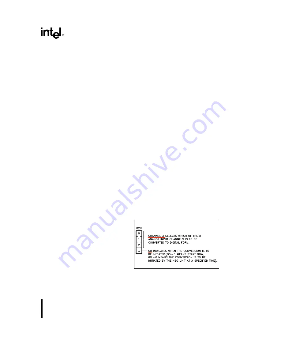
Conversions are started by loading the ADÐCOM-
MAND register at location 02H with the channel num-
ber. The conversion can be started immediately by set-
ting the GO bit to a one. If it is cleared the conversion
will start when the HSO unit triggers it. The A/D com-
mand register must be written to for each conversion,
even if the HSO is used as the trigger. The result of
the conversion is read in the ADÐRESULT(High)
and ADÐRESULT(Low) registers. The ADÐRE-
SULT(High) contains the most significant eight bits of
the conversion. The ADÐRESULT(Low) register con-
tains the remaining two bits and the A/D channel num-
ber and A/D status. The format for the ADÐCOM-
MAND register is shown in Figure 11-1. In Window
15, reading the ADÐCOMMAND register will read
the last command written. Writing to the ADÐRE-
SULT register will write a value into the result register.
270651 – 33
Figure 11-1. A/D Command Register
51
数控原理与维修
http://www.agreenleaf.cn
Содержание 80C196KB Series
Страница 1: ...November 1990 80C196KB User s Guide Order Number 270651 003 http www agreenleaf cn...
Страница 59: ...80C196KB USER S GUIDE Figure 11 7 Ideal A D Characteristic 270651 37 55 http www agreenleaf cn...
Страница 60: ...80C196KB USER S GUIDE Figure 11 8 Actual and Ideal Characteristics 270651 38 56 http www agreenleaf cn...
Страница 61: ...80C196KB USER S GUIDE Figure 11 9 Terminal Based Characteristic 270651 39 57 http www agreenleaf cn...
Страница 70: ...80C196KB USER S GUIDE Figure 13 5 Reset Sequence 80C196KB Reset Sequence 270651 45 66 http www agreenleaf cn...
Страница 83: ...80C196KB USER S GUIDE 270651 80 Figure 15 14 AC Timing Diagrams 79 http www agreenleaf cn...
Страница 84: ...80C196KB USER S GUIDE 270651 81 270651 84 Figure 15 14 AC Timing Diagrams Continued 80 http www agreenleaf cn...