4-6
4
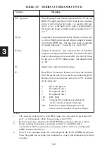
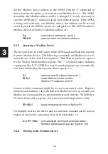
In the 4819A, the RAM is a 8 bit wide memory that is primarily used for
data storage, operating variables and configuration settings. The 4819A
data buffers are several times larger than any anticipated message so no
data loss ever occurs. GPIB bus data is never lost since the 4819A simply
inhibits further Bus handshakes until there is room in the GPIB buffer for
more data.
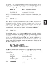
The 4819A has an on-card regulator that converts unreg5.5 to +12
volt DC power to +5 Vdc to run the 4819A's circuits. A jumper on the
4819A bypasses the regulator so that the 4819A can be run from regulated
5 volt DC power. A DC-DC converter in the RS-232 transmitter IC makes
the ± 9 Vdc necessary to power the RS-232 drivers.
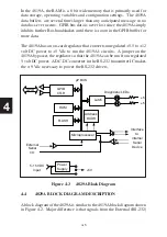
GPIB
CTLR
RAM
Microprocessor
Address
DCDR
µP BUS
+5
FLASH
Interface
to
internal
Serial
Device
Power
Supply
5-15 VDC
Input
+5V
Latch
GPIB
+5
Diagnostic LEDs
External
Serial
I/O
Figure 4-3 4829A Block Diagram
4.4
4829A BLOCK DIAGRAM DESCRIPTION
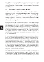
A block diagram of the 4829A is similar to the 4819A block diagram shown
in Figure 4-2. Major difference is that signals from the External (RS-232)
Содержание 4809A
Страница 5: ...ii This page left intentionally blank...
Страница 51: ...2 30 2 This page left intentionally blank...
Страница 89: ...4 8 4 This page intentionally left blank...
Страница 99: ...5 10 5 This page left intentionally blank...
Страница 125: ...A 26 A3 This page intentionally left blank...
Страница 131: ...I Index 6 This page left intentionally blank...

