


4-3
4
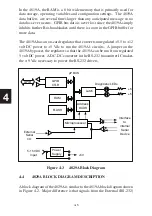
received message are counted and verified against the expected response
character count. The message is then checksumed. If the received message
is a valid response, any data is converted in to the correct format and placed
in the GPIB buffer where can be transferred out onto the GPIB bus when
the unit is next address to talk. Messages that contain errors or Exception
messages cause the 4899A to set bits in the Questionable Register and to
place an error value in the Modbus Error Register. The 4899A contains a
multilevel Status Byte Register and Event Register structure enables the
4899A to generate a Service Request and interrupt the GPIB bus controller
when errors are detected.
Flash Memory contains all of the 4899A's program instructions, command
tables, and power turn-on/self test routines. At power turn-on, the 4899A
performs a self test on each functional block to determine whether there is
a gross system failure. Any self test error is displayed as a pattern of blink-
ing LEDs on the front panel. The error pattern is repeated until the unit is
turned off. Just after completing the self test routine, the 4899A displays its
current GPIB address setting on the front panel LEDs. Bit weights are read
from right to left with the least significant bit on the far right. The RDY
LED comes on to indicate a successful completion of the self test routine.
The 4899A's and 4809A's configuration settings, serial number and other
parameters that are subject to change are saved in a nonvolatile Flash sec-
tor. At power on time, the microprocessor copies the saved configuration
to RAM where it is used to operate the unit. Any changes made to the set-
tings during run time are not stored in the Flash sector until the user sends
the 4899A the *SAV 0
command.
In the 4899A, the RAM is a 8 bit wide memory that is primarily used for
data storage, operating variables and configuration settings. The 4899A
data buffers are mechanized as straight buffers because of the Modbus
command-response protocol. The buffers are several times larger than any
anticipated message so no data loss ever occurs. GPIB bus data is never
lost since the 4899A simply inhibits further Bus handshakes until there is
room in the GPIB buffer for more data.
The 4899A's power supply is a switching regulator that converts a unregu-
lated 9 to 32 volt DC input to +5 Vdc to run the 4899A's internal logic
chips. A DC-DC converter in the RS-232 transmitter IC makes ± 9 Vdc to
operate the RS-232 drivers.
Содержание 4809A
Страница 5: ...ii This page left intentionally blank...
Страница 51: ...2 30 2 This page left intentionally blank...
Страница 89: ...4 8 4 This page intentionally left blank...
Страница 99: ...5 10 5 This page left intentionally blank...
Страница 125: ...A 26 A3 This page intentionally left blank...
Страница 131: ...I Index 6 This page left intentionally blank...