4-5
4
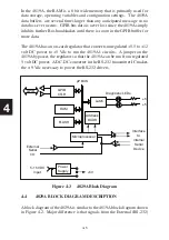
connector and to the GPIB logic. Because of the simple OR gate path, only
one interface can be used to control the Modbus device at a time.
The Flash memory contains all of the 4819A's program instructions, com-
mand tables, and power turn-on/self test routines. At power turn-on, the
4819A performs a self test on each functional block to determine whether
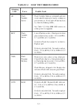
there is a gross system failure. Any self test error is displayed as a pattern
of blinking LEDs on the front panel. The error pattern is repeated until
the unit is turned off. Just after completing the self test routine, the 4819A
displays its current GPIB address setting on its LEDs. The RDY LED comes
on to indicate a successful completion of the self test routine.
The Flash also contains all of the 4819A's configuration settings, serial
number and other parameters that are subject to change. At power on time,
the microprocessor copies the configuration from Flash memory to RAM
where it is used to operate the unit. Any changes made to the settings dur-
ing run time are not stored in the Flash memory until saved with the *SAV
0
command.
Figure 4-2 4819A Block Diagram
Содержание 4809A
Страница 5: ...ii This page left intentionally blank...
Страница 51: ...2 30 2 This page left intentionally blank...
Страница 89: ...4 8 4 This page intentionally left blank...
Страница 99: ...5 10 5 This page left intentionally blank...
Страница 125: ...A 26 A3 This page intentionally left blank...
Страница 131: ...I Index 6 This page left intentionally blank...

