MB95630H Series
44
FUJITSU SEMICONDUCTOR LIMITED
MN702-00009-1v0-E
CHAPTER 3 CLOCK CONTROLLER
3.5 Operations in Low Power Consumption
Mode (Standby Mode)
■
Standby Mode State Transition Diagram (with Deep Standby Mode Disabled)
Figure 3.5-1 shows a standby mode state transition diagram (with deep standby mode
disabled).
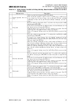
Figure 3.5-1 Standby Mode State Transition Diagram (with Deep Standby Mode Disabled)
Power on
Re
s
et
s
t
a
te
Norm
a
l
(RUN)
s
t
a
te
W
a
tch mode
M
a
in clock/m
a
in CR clock/
m
a
in CR PLL clock/
sub
clock/
sub
-CR clock o
s
cill
a
tion
s
t
ab
iliz
a
tion w
a
it time
Time-
bas
e
timer mode
S
top mode
S
leep mode
(1)
(2)
(
3
)
(5)
(6)
A re
s
et occ
u
r
s
in
a
ny
s
t
a
te.
<1>
(4)
(
8
)
(7)
M
a
in CR clock
o
s
cill
a
tion
s
t
ab
iliz
a
tion
w
a
it time
+
sub
-CR clock
o
s
cill
a
tion
s
t
ab
iliz
a
tion
w
a
it time
Table 3.5-1
Table of State Transition with Deep Standby Mode Disabled (Transition to and
from Standby Mode) (1 / 2)
State transition
Description
<1>
Normal operation after reset
state
After a reset, the device transits to main CR clock mode.
If the reset that has occurred is a power-on reset, a watchdog reset, a software reset,
or an external reset, the device always wait for the main CR clock oscillation
stabilization wait time and the sub-CR clock oscillation stabilization wait time to
elapse.
(1)
Sleep mode
The device transits to sleep mode when "1" is written to the sleep bit in the standby
control register (STBC:SLP).
(2)
The device returns to the RUN state in response to an interrupt from a peripheral
resource.
(3)
Stop mode
The device transits to stop mode when "1" is written to the stop bit in the standby
control register (STBC:STP).
(4)
In response to an external interrupt, after waiting for the elapse of the oscillation
stabilization wait time required according to the current clock mode, the device
returns to the RUN state.
(5)
Time-base timer mode
The device transits to time-base timer mode when "1" is written to the watch bit in
the standby control register (STBC:TMD) in main clock mode, main CR clock mode,
or main CR PLL clock mode.
(6)
The device returns to the RUN state in response to an interrupt from a peripheral
resource.
Содержание MB95630H Series
Страница 2: ......
Страница 4: ......
Страница 8: ...iv ...
Страница 20: ...xvi ...
Страница 106: ...MB95630H Series 86 FUJITSU SEMICONDUCTOR LIMITED MN702 00009 1v0 E CHAPTER 6 I O PORT 6 2 Configuration and Operations ...
Страница 282: ...MB95630H Series 262 FUJITSU SEMICONDUCTOR LIMITED MN702 00009 1v0 E CHAPTER 14 LIN UART 14 8 Notes on Using LIN UART ...
Страница 642: ...MB95630H Series 622 FUJITSU SEMICONDUCTOR LIMITED MN702 00009 1v0 E APPENDIX A Instruction Overview A 5 Instruction Map ...
Страница 644: ......

