MB95630H Series
MN702-00009-1v0-E
FUJITSU SEMICONDUCTOR LIMITED
231
CHAPTER 14 LIN-UART
14.6 Operations of LIN-UART and LIN-UART
Setting Procedure Example
14.6.3
Operations of LIN function (Operating Mode 3)
In operating mode 3, the LIN-UART works as the LIN master and the LIN slave.
In operating mode 3, the communication format is set to 8-bit data, no parity,
stop bit 1, LSB first.
■
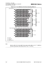
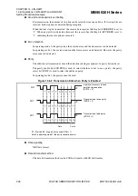
Asynchronous LIN Mode Operation
●
Operation as LIN master
In LIN mode, the master determines the baud rate for the entire bus, and the slave synchronizes
with the master.
Writing "1" to the LBR bit in the LIN-UART extended communication control register
(ECCR) outputs 13 bits to 16 bits at the "L" level from the SOT pin. These bits are the LIN
synch break indicating the beginning of a LIN message.
The TDRE bit in the LIN-UART serial status register (SSR) is then set to "0". After the LIN
synch break, the TDRE bit is set to "1" (initial value). If the TIE bit in SSR is "1" at this time, a
transmit interrupt is output.
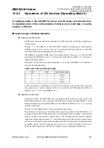
The length of the LIN synch break transmitted is set by the LBL0/LBL1 bits in ESCR as
shown in the following table.
A LIN synch field is transmitted as byte data 0x55 following a LIN synch break. To prevent
the generation of a transmit interrupt, 0x55 can be written to the TDR after the LBR bit in
ECCR is set to "1" even if the TDRE bit is "0".
●
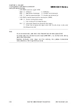
Operation as LIN slave
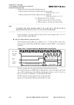
In LIN slave mode, the LIN-UART must synchronize with the baud rate of the master. The
LIN-UART generates a receive interrupt when LIN break interrupt is enabled (LBIE = 1) even
though reception has been disabled (RXE = 0). The LBD bit in ESCR is set to "1" as a receive
interrupt is generated.
Writing "0" to the LBD bit clears the receive interrupt request flag.
The calculation of baud rate is illustrated below using the operation of the LIN-UART as an
example. When the LIN-UART detects the first falling edge of the synch field, set the internal
signal to be input to the 8/16-bit composite timer to "H", and then start the 8/16-bit composite
timer. The internal signal becomes "L" at the fifth falling edge. The 8/16-bit composite timer
must be set to the input capture mode. In addition, the 8/16-bit composite timer interrupt must
be enabled and the 8/16-bit composite timer must be set to detect both edges. The time at
which the input signal input to the 8/16-bit composite timer is eight times the baud rate.
Table 14.6-3 LIN Synch Break Length
LBL0
LBL1
Synch break length
0
0
13 bits
1
0
14 bits
0
1
15 bits
1
1
16 bits
Содержание MB95630H Series
Страница 2: ......
Страница 4: ......
Страница 8: ...iv ...
Страница 20: ...xvi ...
Страница 106: ...MB95630H Series 86 FUJITSU SEMICONDUCTOR LIMITED MN702 00009 1v0 E CHAPTER 6 I O PORT 6 2 Configuration and Operations ...
Страница 282: ...MB95630H Series 262 FUJITSU SEMICONDUCTOR LIMITED MN702 00009 1v0 E CHAPTER 14 LIN UART 14 8 Notes on Using LIN UART ...
Страница 642: ...MB95630H Series 622 FUJITSU SEMICONDUCTOR LIMITED MN702 00009 1v0 E APPENDIX A Instruction Overview A 5 Instruction Map ...
Страница 644: ......


