MB95630H Series
518
FUJITSU SEMICONDUCTOR LIMITED
MN702-00009-1v0-E
CHAPTER 24 I
2
C BUS INTERFACE
24.7 Registers
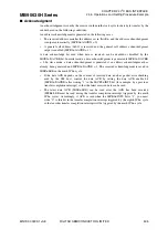
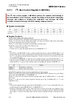
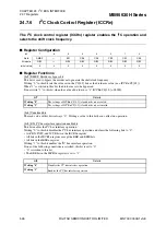
[bit5] SCC: START condition generation bit
This bit generates a repeated START condition to restart communications in master mode.
In master mode, writing "1" to this bit generates a repeated START condition.
Writing "0" to this bit has no effect on operation.
Notes:
• Do not set this bit to "1" or the IBCR1n:MSS bit to "0" at the same time.
• With the IBCR1n:INT bit set to "0", an attempt to write "1" to the SCC bit is ignored (no START condition
is generated). In addition, with the INT bit set to "1", when writing "1" to the SCC bit and writing "0" to the
INT bit occur simultaneously, writing "1" to the SCC bit is given priority.
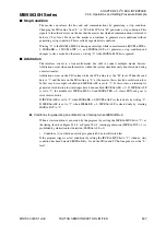
[bit4] MSS: Master/slave select bit
This bit selects an operation mode from master mode and slave mode.
Writing "1" to this bit while the I
2
C bus is in the idle state (IBSRn:BB = 0) selects master mode, generates a
START condition, and then starts address transfer.
Writing "0" to the bit while the I2C bus is in the busy state (IBSRn:BB = 1) selects slave mode, generates a
STOP condition, and then terminates data transfer.
When an arbitration lost occurs during data or address transfer in master mode, this bit is cleared to "0" and
the operation mode switches to slave mode.
Notes:
• Do not set this bit to "0" or the SCC bit to "1" at the same time.
• With the INT bit set to "0", an attempt to write "0" to the MSS bit is ignored. With the INT bit set to "1’, when
writing "0" to the MSS bit and writing "0" to the INT bit occur simultaneously, writing "0" to the MSS bit is
given priority.
• In slave mode, during transmission or reception, writing "1" to the MSS bit does not set the ALF bi to "1".
Do not write "1" to the MSS bit during transmission or reception in slave mode.
[bit3] DACKE: Data acknowledge enable bit
This bit controls the data acknowledge in data reception.
Writing "0" to this bit disables data acknowledge output.
Writing "1" to this bit enables data acknowledge output. In master mode, with this bit set to "1", a data
acknowledge is output in the ninth SCLn cycle during data reception. In slave mode, a data acknowledge is
output in the ninth SCLn cycle only when an address acknowledgment has already been output.
bit5
Details
Read access
The read value is always "0".
Writing "0"
Has no effect on operation.
Writing "1"
Generates a repeated START condition in master mode.
bit4
Details
Writing "0"
Slave mode
Writing "1"
Master mode
bit3
Details
Writing "0"
Disables data acknowledge output.
Writing "1"
Enables data acknowledge output.
Содержание MB95630H Series
Страница 2: ......
Страница 4: ......
Страница 8: ...iv ...
Страница 20: ...xvi ...
Страница 106: ...MB95630H Series 86 FUJITSU SEMICONDUCTOR LIMITED MN702 00009 1v0 E CHAPTER 6 I O PORT 6 2 Configuration and Operations ...
Страница 282: ...MB95630H Series 262 FUJITSU SEMICONDUCTOR LIMITED MN702 00009 1v0 E CHAPTER 14 LIN UART 14 8 Notes on Using LIN UART ...
Страница 642: ...MB95630H Series 622 FUJITSU SEMICONDUCTOR LIMITED MN702 00009 1v0 E APPENDIX A Instruction Overview A 5 Instruction Map ...
Страница 644: ......


