MB95630H Series
MN702-00009-1v0-E
FUJITSU SEMICONDUCTOR LIMITED
563
CHAPTER 25 DUAL OPERATION FLASH MEMORY
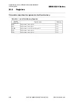
25.8 Registers
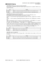
[bit2] IRQEN: Flash memory program/erase interrupt enable bit
This bit enables or disables the generation of interrupt requests triggered by the completion of Flash memory
programming/erasing.
[bit1] WRE: Flash memory program/erase enable bit
This bit enables or disables the programming/erasing of data into/from the Flash memory area.
Set the WRE bit before invoking a Flash memory program/erase command.
Writing "0" to this bit disables generating program/erase signals even when a program/erase command is
input.
Writing "1" to this bit enables programming/erasing Flash memory data after a program/erase command is
input.
When not programming data into or erasing data from the Flash memory, set the WRE bit to "0" in order to
prevent data from being accidentally written into or erased from the Flash memory.
To program data to the Flash memory, set FSR:WRE to "1" to enable programming data to the Flash
memory, and set the flash memory sector write control register 0 (SWRE0) according to the Flash memory
sector into which data is to be written. When Flash memory programming is disabled (FSR:WRE = 0), no
write access to a sector in the Flash memory can be executed even though it has been enabled by setting a bit
corresponding to that sector in the Flash memory sector write control register 0 (SWRE0) to "1".
[bit0] SSEN: Sector swap enable bit
This bit is used to swap part of SA2 in the upper bank, at which interrupt vectors are kept, for SA1 in the
lower bank.
bit2
Details
Writing "0"
Disables generating an interrupt upon completion of Flash memory programming/erasing.
Writing "1"
Enables generating an interrupt upon completion of Flash memory programming/erasing.
bit1
Details
Writing "0"
Disables Flash memory area programming/erasing.
Writing "1"
Enables Flash memory area programming/erasing.
bit0
Details
Writing "0"
Maps SA1 to 0x1800-0x1FFF, and the 2 Kbyte address area of SA2 to 0xF800-0xFFFF.
Writing "1"
Maps the 2 Kbyte address area of SA2 to 0x1800-0x1FFF, and SA1 to 0xF800-0xFFFF.
Содержание MB95630H Series
Страница 2: ......
Страница 4: ......
Страница 8: ...iv ...
Страница 20: ...xvi ...
Страница 106: ...MB95630H Series 86 FUJITSU SEMICONDUCTOR LIMITED MN702 00009 1v0 E CHAPTER 6 I O PORT 6 2 Configuration and Operations ...
Страница 282: ...MB95630H Series 262 FUJITSU SEMICONDUCTOR LIMITED MN702 00009 1v0 E CHAPTER 14 LIN UART 14 8 Notes on Using LIN UART ...
Страница 642: ...MB95630H Series 622 FUJITSU SEMICONDUCTOR LIMITED MN702 00009 1v0 E APPENDIX A Instruction Overview A 5 Instruction Map ...
Страница 644: ......


