MB95630H Series
MN702-00009-1v0-E
FUJITSU SEMICONDUCTOR LIMITED
469
CHAPTER 22 UART/SIO
22.6 Operations and Setting Procedure Example
The TDRE bit is set at the point indicated in the following figure if the preceding piece of
transmit data does not exist in the transmission shift register.
Figure 22.6-7 Setting Timing 1 for Transmit Data Register Empty Flag Bit (TDRE)
(When TXE is "1")
Figure 22.6-8 Setting Timing 2 for Transmit Data Register Empty Flag Bit (TDRE)
(When TXE Is Switched from "0" to "1")
●
Concurrent transmission and reception
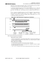
In asynchronous clock mode (UART), transmission and reception can be performed
independently. Therefore, transmission and reception can be performed at the same time or
even with transmitting and receiving frames overlapping each other in shifted phases.
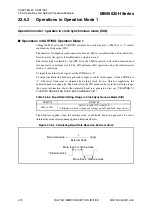
UOn
D0
D1
TDRE
Tr
a
n
s
mit
interr
u
pt
TXE = “1”
Writing of
tr
a
n
s
mit d
a
t
a
D2
D
3
D
a
t
a
tr
a
n
s
fer from UART/
S
IO
s
eri
a
l o
u
tp
u
t d
a
t
a
regi
s
ter (TDRn) to tr
a
n
s
mi
ss
ion
s
hift regi
s
ter i
s
performed in one m
a
chine clock (MCLK) cycle.
D0
D1
D2
D
3
UOn
TDRE
Tr
a
n
s
mit
interr
u
pt
TXE
Writing of
tr
a
n
s
mit d
a
t
a
Содержание MB95630H Series
Страница 2: ......
Страница 4: ......
Страница 8: ...iv ...
Страница 20: ...xvi ...
Страница 106: ...MB95630H Series 86 FUJITSU SEMICONDUCTOR LIMITED MN702 00009 1v0 E CHAPTER 6 I O PORT 6 2 Configuration and Operations ...
Страница 282: ...MB95630H Series 262 FUJITSU SEMICONDUCTOR LIMITED MN702 00009 1v0 E CHAPTER 14 LIN UART 14 8 Notes on Using LIN UART ...
Страница 642: ...MB95630H Series 622 FUJITSU SEMICONDUCTOR LIMITED MN702 00009 1v0 E APPENDIX A Instruction Overview A 5 Instruction Map ...
Страница 644: ......


