MB95630H Series
428
FUJITSU SEMICONDUCTOR LIMITED
MN702-00009-1v0-E
CHAPTER 21 MULTI-PULSE GENERATOR
21.6 Registers
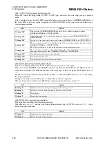
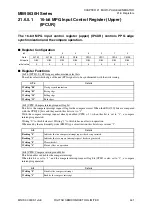
[bit4:2] OPS[2:0]: Data transfer method select bits
These bits control the output timing of OPT5 to OPT0 pins and select the write timing control operation
mode.
Data is transferred from the 16-bit MPG output data buffer register (upper/lower) (OPDBRHx/OPDBRLx) to
the 16-bit MPG output data register (upper/lower) (OPDUR/OPDLR) at the write timing controlled by the
selected operation mode.
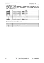
[bit1] WTIF: Write timing interrupt request flag bit
This bit is an interrupt request flag for the output timing switch set by a write signal.
When data in the OPDBRHx and OPDBRLx registers specified by the BNKF bit and RDA[2:0] bits in
OPDUR is transferred to OPDUR and OPDLR at the rising edge of the write signal, the WTIF bit is set to
"1".
With the write timing interrupt already enabled (WTIE = 1), when the WTIF bit is set to "1", a write timing
interrupt is generated.
Writing "0" to this bit clears it. Writing "1" to this bit has no effect on operation.
When read by the read-modify-write (RMW) type of instruction, this bit always returns "1".
[bit0] WTIE: Write timing interrupt enable bit
This bit enables or disables the write timing interrupt.
When this bit is set to "1", and the write timing interrupt request flag bit (WTIF) is also set to "1", a write
timing interrupt is generated.
bit4:2
Details
Writing "000"
Data is written to OPDBRHx/OPDBRLx by the software, and then is transferred from
OPDBRHx/OPDBRLx to OPDUR/OPDLR.
Writing "001"
An underflow in the 16-bit reload timer triggers data transfer from OPDBRHx/OPDBRLx to
OPDUR/OPDLR.
Writing "010"
Position detection input triggers data transfer from OPDBRHx/OPDBRLx to OPDUR/OPDLR.
Writing "011"
The write signal generated by an underflow in the 16-bit reload timer triggers data transfer from
OPDBRHx/OPDBRLx to OPDUR/OPDLR.
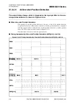
The 16-bit reload timer is started by the position detection comparison circuit
Writing "100"
The write signal generated by either an underflow in the 16-bit reload timer or position detection
input triggers data transfer from OPDBRHx/OPDBRLx to OPDUR/OPDLR.
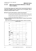
Writing "101"
One-shot position detection or timer underflow
Writing "110"
One-shot position detection
Writing "111"
One-shot position detection and timer underflow
bit1
Details
Reading "0"
Indicates that no write timing interrupt request has been generated.
Reading "1"
Indicates that a write timing interrupt request has been generated.
Writing "0"
Clears this bit.
Writing "1"
Has no effect on operation.
bit0
Details
Writing "0"
Disables the write timing interrupt.
Writing "1"
Enables the write timing interrupt.
Содержание MB95630H Series
Страница 2: ......
Страница 4: ......
Страница 8: ...iv ...
Страница 20: ...xvi ...
Страница 106: ...MB95630H Series 86 FUJITSU SEMICONDUCTOR LIMITED MN702 00009 1v0 E CHAPTER 6 I O PORT 6 2 Configuration and Operations ...
Страница 282: ...MB95630H Series 262 FUJITSU SEMICONDUCTOR LIMITED MN702 00009 1v0 E CHAPTER 14 LIN UART 14 8 Notes on Using LIN UART ...
Страница 642: ...MB95630H Series 622 FUJITSU SEMICONDUCTOR LIMITED MN702 00009 1v0 E APPENDIX A Instruction Overview A 5 Instruction Map ...
Страница 644: ......

