background image

S1C6S3N2 TECHNICAL HARDWARE

EPSON

I-97

CHAPTER 5: SUMMARY OF NOTES

SUMMARY OF NOTES

Notes for Low Current Consumption

The S1C6S3N2 Series contains control registers for each of

the circuits so that current consumption can be lowered.

These control registers lower the current consumption

through programs that operate the circuits at the minimum

levels.

The following text explains the circuits that can control

operation and their control registers.  Refer to these when

putting programs together.

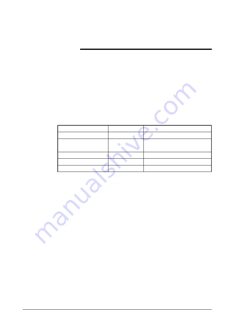
Table 5.1.1  Circuits and control registers

CHAPTER 5

5.1

Below are the circuit statuses at initial reset.

CPU:

Operating status

CPU operating frequency:

Low speed side (CLKCHG = "0"),

OSC3 oscillation circuit stop

status (OSCC = "0")

Heavy load protection mode: Normal operating mode

(HLMOD = "0")

SVD circuit:

OFF status (HLMOD = "0", BLS = "0")

Analog comparator:

OFF status (AMPON = "0")

Also, be careful about panel selection because the current

consumption can differ by the order of several µA on ac-

count of the LCD panel characteristics.

Circuits (and Items)

CPU

CPU operation frequency

(S1C6S3A2)

Heavy load protection mode

SVD circuit

Analog comparator

Control Registers

HALT instruction

CLKCHG, OSCC

HLMOD

HLMOD, BLS

AMPON

Order of Consumed Current

See electrical characteristics (Chapter 7)

See electrical characteristics (Chapter 7)

See electrical characteristics (Chapter 7)

Severral tens 

µ

A

Severral tens 

µ

A

Содержание S1C6S3N2

Страница 1: ...MF859 06 Technical Manual CMOS 4 BIT SINGLE CHIP MICROCOMPUTER S1C6S3N2 Technical Hardware S1C6S3N2 Technical Software S1C6S3N2 ...

Страница 2: ...uiring high level reliability such as medical products Moreover no license to any intellectual property rights is granted by implication or otherwise and there is no representation or warranty that anything made in accordance with this material will be free from any patent or copyright infringement of a third party This material or portions thereof may contain technology or the subject relating to...

Страница 3: ... software of the S1C6S3N2 I S1C6S3N2 Technical Hardware This part explains the function of the S1C6S3N2 the circuit configu rations and details the controlling method II S1C6S3N2 Technical Software This part explains the programming method of the S1C6S3N2 Software Hardware ...

Страница 4: ......

Страница 5: ...1C6N3B0 S1C62440 S1C624A0 S1C6S460 Previous No E0C6247 E0C6248 E0C6S48 E0C624C E0C6251 E0C6256 E0C6292 E0C6262 E0C6266 E0C6274 E0C6281 E0C6282 E0C62M2 E0C62T3 New No S1C62470 S1C62480 S1C6S480 S1C624C0 S1C62N51 S1C62560 S1C62920 S1C62N62 S1C62660 S1C62740 S1C62N81 S1C62N82 S1C62M20 S1C62T30 Comparison table between new and previous number of development tools Development tools for the S1C60 62 Fam...

Страница 6: ......

Страница 7: ...Hardware Hardware S1C6S3N2 I Technical Hardware ...

Страница 8: ......

Страница 9: ...et pin RESET I 11 Simultaneous high input to input ports K00 K03 I 11 Watchdog timer Auxiliary reset I 11 Oscillation detection circuit Auxiliary reset I 12 Internal register at initial setting I 12 2 3 Test Terminal TEST I 12 CHAPTER 3 CPU ROM RAM I 13 3 1 CPU I 13 3 2 ROM I 14 3 3 RAM I 15 CHAPTER 4 PERIPHERAL CIRCUITS AND OPERATION I 16 4 1 Memory Map I 16 4 2 Resetting Watchdog Timer I 24 Conf...

Страница 10: ...put Ports R00 R03 R10 R13 I 40 Configuration of output ports I 40 Mask option I 40 Control of output ports I 43 Programming note I 45 4 6 I O Ports P00 P03 P10 P13 I 46 Configuration of I O ports I 46 I O control register and I O mode I 47 Mask option I 47 Control of I O ports I 48 Programming notes I 50 4 7 LCD Driver COM0 3 SEG0 37 I 51 Configuration of LCD driver I 51 Switching between dynamic ...

Страница 11: ...te I 76 4 11 Analog Comparator I 77 Configuration of analog comparator I 77 Operation of analog comparator I 77 Control of analog comparator I 78 Programming notes I 79 4 12 Supply Voltage Detection SVD Circuit and Heavy Load Protection Function I 80 Configuration of SVD circuit I 80 Heavy load protection function I 81 Detection timing of SVD circuit I 82 Control of SVD circuit I 84 Programing not...

Страница 12: ...ER 7 ELECTRICAL CHARACTERISTICS I 107 7 1 Absolute Maximum Rating I 107 7 2 Recommended Operating Conditions I 108 7 3 DC Characteristics I 109 7 4 Analog Circuit Characteristics and Consumed Current I 111 7 5 Oscillation Characteristics I 119 CHAPTER 8 PACKAGE I 124 8 1 Plastic Package I 124 8 2 Ceramic Package for Test Samples I 126 CHAPTER 9 PAD LAYOUT I 127 9 1 Diagram of Pad Layout I 127 9 2 ...

Страница 13: ...ystems Furthermore the S1C6S3N2 is a shrunk model of the S1C62N32 It can be used as various controller applications such as a clock game and pager Configuration The S1C6S3N2 Series is configured as follows depending on supply voltage and oscillation circuits Model S1C6S3N2 S1C6S3L2 S1C6S3B2 S1C6S3A2 Supply Voltage 1 8 3 6 V 0 9 1 8 V 0 9 3 6 V 1 8 3 6 V External Supports Supports Not Supports LCD ...

Страница 14: ...ecuted Crystal oscillation circuit 32 768 kHz Typ No setting 100 types 153 µsec 214 µsec 366 µsec CLK 32 768 kHz 2 048 words 12 bits per word 144 words 4 bits per word 5 bits pull down resistor can be added through mask option 8 bits BZ BZ FOUT outputs are available through mask option 8 bits pull down resistor is added during input data read out Either 38 segments 4 or 3 or 2 common 1 V 3V 1 4 or...

Страница 15: ...troller LCD Driver Interrupt Generator Core CPU S1C6200A OSC System Reset Control COM0 COM3 SEG0 SEG37 VDD VL1 VL3 CA CB VS1 VSS K00 K03 K10 TEST P00 P03 R00 R03 P10 P13 R10 R13 AMPP AMPM RESET OSC1 OSC2 OSC3 OSC4 RAM 144 x 4 ROM 2 048 x 12 Event Counter SVD I Port I O Port O Port Comparator Timer Stop Watch ...

Страница 16: ...SEG9 SEG10 SEG11 SEG12 SEG13 SEG14 SEG15 SEG16 Pin No Pin Name N C No connection QFP14 80pin 1 2 3 4 5 6 7 8 9 10 11 12 13 14 15 16 17 18 19 20 AMPP AMPM K10 K03 K02 K01 K00 P03 P02 P01 P00 P13 P12 P11 P10 R03 R02 R01 R00 R12 Pin No 21 22 23 24 25 26 27 28 29 30 31 32 33 34 35 36 37 38 39 40 R11 R10 R13 VSS RESET OSC4 OSC3 VS1 OSC2 OSC1 VDD VL3 VL2 VL1 N C CB CA COM3 COM2 COM1 Pin No 41 42 43 44 4...

Страница 17: ... terminal Constant voltage output terminal for oscillation Function Crystal oscillator input terminal Crystal oscillator output terminal 1 2 Input terminal Input output terminal Output terminal Output terminal Can output BZ through mask option Output terminal Can output BZ through mask option Output terminal Output terminal Can output FOUT through mask option Analog comparator noninverted input te...

Страница 18: ... Or the S1C6S3N2 Series generates the necessary internal voltage with the regulated voltage circuit VS1 for oscillators VL2 for LCDs and the voltage booster circuit VL1 VL3 for LCDs Figures 2 1 1 a and 2 1 1 b show the configuration of power supply 1 Supply voltage 6S3N2 1 8 2 2 3 6 V 6S3L2 0 9 1 8 V 6S3B2 0 9 3 6 V 6S3A2 1 8 2 2 3 6 V The values enclosed with are mini mum voltages for application...

Страница 19: ...1 VL2 VL3 CA CB VSS OSC1 4 COM0 3 SEG0 37 VL1 VL2 VL3 C5 C2 C3 C4 C1 Fig 2 1 1 a Example of configuration of power supply S1C6S3L2 6S3B2 External power supply Internal circuit Oscillation circuit LCD driver circuit LCD system voltage booster reducer circuit Oscillation system regulated voltage circuit LCD system regulated voltage circuit VDD VS1 VS1 VL2 VL2 VL1 VL3 CA CB VSS OSC1 4 COM0 3 SEG0 37 ...

Страница 20: ...ystem regulated voltage circuit therefore the external capacitors are required Figure 2 1 2 shows the external elements when the the LCD sys tem regulated voltage circuit is not used S1C6S3A2 4 5 V LCD panel 1 4 1 3 1 2 duty 1 3 bias Note VL2 is shorted to VSS inside the IC S1C6S3N2 S1C6S3A2 3 V LCD panel 3 V LCD panel 1 4 1 3 1 2 duty 1 3 bias 1 4 1 3 1 2 duty 1 2 bias Note VL3 is shorted to VSS ...

Страница 21: ... selection of the LCD system power supply When external is selected by the mask option the specified LCD drive voltage terminal is connected to the VSS inside the IC Combinations that are marked with an cannot be selected 1 3 Bias Internal VL1 VSS VL1 VL2 3 0 V LCD 3 0 V LCD 3 0 V LCD 3 0 V LCD S1C6S3N2 S1C6S3A2 S1C6S3L2 S1C6S3B2 External VL2 VSS 4 5 V LCD VL3 VSS 3 0 V LCD 3 0 V LCD 1 2 Bias Inte...

Страница 22: ...nal initial reset by the RESET terminal 2 External initial reset by simultaneous high input to terminals K00 K03 3 Initial reset by watchdog timer 4 Initial reset by the oscillation detection circuit The IC is reset after 1 sec has elapsed from a start of oscillation Figure 2 2 1 shows the configuration of the initial reset circuit 2 2 Fig 2 2 1 Configuration of initial reset circuit Vss RESET K03...

Страница 23: ... a noise rejector circuit Table 2 2 1 shows the combinations of input ports K00 K03 that can be selected with the mask option Reset pin RESET Simultaneous high input to input ports K00 K03 Table 2 2 1 Input port combinations A Not used B K00 K01 C K00 K01 K02 D K00 K01 K02 K03 When for instance mask option D K00 K01 K02 K03 is selected initial reset is executed when the signals input to the four p...

Страница 24: ... peripheral circuit 4 1 Table 2 2 2 Initial values 2 3 The oscillation detection circuit outputs the initial reset signal at power on until the crystal oscillation circuit OSC1 begins oscillating or when this crystal oscillation circuit OSC1 halts oscillating for some reason However depending on the power on sequence voltage rise timing the circuit may not work properly Therefore use the reset ter...

Страница 25: ... 6200A Core CPU Manual for details about the S1C6200A Note the following points with regard to the S1C6S3N2 Series 1 The SLEEP operation is not assumed so the SLP instruc tion cannot be used 2 Because the ROM capacity is 2 048 words bank bits are unnecessary and PCB and NBP are not used 3 The RAM page is set at 0 only so that the page part XP YP of the index register that performs address specific...

Страница 26: ...ach The program area is 8 pages 0 7 each of 256 steps 00H FFH After initial reset the program beginning address is page 1 step 00H The interrupt vector is allocated to page 1 steps 01H 0FH 0page 00H step Program start address 1page 2page 3page 4page 5page 6page 7page 01H step 0FH step 10H step FFH step 12 bits Interrupt vector area Fig 3 2 1 ROM configuration ...

Страница 27: ...ry can be used as stack area when saving subroutine calls and registers so be careful not to overlap the data area and stack area 2 Subroutine calls and interrupts take up three words of the stack area 3 The data memory 000H 00FH is for the register pointers RP and is the addressable memory register area 4 The data memory is split into two areas 000H 06FH and 080H 09FH so take care when allocating...

Страница 28: ...be how the peripheral circuits operation Memory Map Data memory of the S1C6S3N2 Series has an address space of 160 words of which 48 words are allocated to segment data memory and 32 words to I O data memory Figures 4 1 1 and 4 1 2 present the overall memory maps of the S1C6S3N2 Series and Tables 4 1 1 a 4 1 1 f the pe ripheral circuits I O space memory maps 4 1 Address Page High Low 0 1 2 3 4 5 6...

Страница 29: ...abled When C0H EFH is selected write only is enabled If 40H 6FH is assigned RAM is used as the segment area 48 words 3 Memory is not mounted in unused area within the memory map and in memory area not indicated in this chapter For this reason normal operation cannot be assured for programs that have been prepared with access to these areas Note Fig 4 1 2 Memory map segment area Address Page High L...

Страница 30: ...TM1 TM0 0 0 0 0 Timer data clock timer 2 Hz Timer data clock timer 4 Hz Timer data clock timer 8 Hz Timer data clock timer 16 Hz SWL3 SWL2 SWL1 SWL0 0 0 0 0 MSB Stopwatch counter 1 100 sec BCD LSB SWH3 SWH2 SWH1 SWH0 0 0 0 0 K03 K02 K01 K00 2 2 2 2 High High High High Low Low Low Low MSB Stopwatch counter 1 10 sec BCD LSB Input port K00 K03 1 Initial value at the time of initial reset 2 Not set in...

Страница 31: ...rrupt mask register stopwatch 1 Hz Interrupt mask register stopwatch 10 Hz 0 EIK10 DFK10 K10 0 0 2 2 Enable Falling High Mask Rising Low Interrupt mask register K00 K03 R W BLD BLS 0 0 Heavy load Normal ON Normal OFF Heavy load protection mode register R R Unused Interrupt mask register K10 Differential register K10 Input port K10 Low voltage 0 074H DFK03 DFK02 DFK01 DFK00 R W DFK03 DFK02 DFK01 DF...

Страница 32: ...k Mask Mask Interrupt mask register clock timer 2 Hz Interrupt mask register clock timer 8 Hz Interrupt mask register clock timer 32 Hz 0 TI2 TI8 TI32 0 0 0 2 Yes Yes Yes No No No Unused LCD drive switch Interrupt factor flag clock timer 2 Hz Interrupt factor flag clock timer 8 Hz Interrupt factor flag clock timer 32 Hz 0 07AH 07BH IK1 IK0 SWIT1 SWIT0 R03 R01 R00 R 0 0 0 0 Yes Yes Yes Yes No No No...

Страница 33: ...imer reset Stopwatch counter RUN STOP Stopwatch counter reset I O control register 0 P00 P03 2 2 2 2 Output port R13 BZ Output port R12 FOUT Output port R11 Output port R10 BZ R13 TMRST W R W W R W I O port P00 P03 Output latch reset at time of SR Reset RUN Reset Output STOP Input 07FH WDRST WD2 WD1 WD0 R WDRST WD2 WD1 WD0 Reset 0 0 0 5 Reset W Timer data watchdog timer 1 4 Hz Timer data watchdog ...

Страница 34: ...0 2 2 2 2 kHz 4 kHz 0 0 AMPDT AMPON 1 0 2 2 ON OFF EV03 EV02 EV01 EV00 EV07 EV06 EV05 EV04 0 0 0 0 Buzzer frequency selection register Unused Unused Unused Unused Unused Analog comparator data Analog comparator ON OFF R EV07 R Event counter Low order EV00 EV03 Event counter High order EV04 EV07 R W R W 0 0 0 0 0 0 0 0 0 1 Initial value at the time of initial reset 2 Not set in the circuit 3 Undefi...

Страница 35: ...Low Low Low Low 0 CLKCHG OSCC IOC1 0 0 0 OSC3 ON OSC1 OFF Unused CPU clock switch OSC3 oscillator ON OFF I O control register 1 P10 P13 Reset 5 RUN Reset R Unused Event counter RUN STOP Unused Event counter reset R W 2 2 2 2 2 2 2 R W I O port P10 P13 Output latch reset at time of SR R W W STOP P12 P11 P10 CLKCHG Output Input 0 0 0 1 Initial value at the time of initial reset 2 Not set in the circ...

Страница 36: ...low of the MSB Watchdog timer reset processing in the program s main routine enables detection of program overrun such as when the main routine s watchdog timer processing is bypassed Ordinarily this routine is incorporated where periodic processing takes place just as for the timer interrupt rou tine The watchdog timer operates in the halt mode If the halt status continues for 3 or 4 seconds the ...

Страница 37: ...lue at the time of initial reset 2 Not set in the circuit 3 Undefined 4 Reset 0 immediately after being read 5 Constantly 0 when being read This is the bit for resetting the watchdog timer When 1 is written Watchdog timer is reset When 0 is written No operation Read out Always 0 When 1 is written to WDRST the watchdog timer is reset and the operation restarts immediately after this When 0 is writt...

Страница 38: ...esistance as an external element when CR oscillation is selected but when ceramic oscillation is selected both the ceramic oscillator and two capacitors gate and drain capacitance are required Figure 4 3 2 is the block diagram of the OSC3 oscillation circuit 4 3 OSC3 oscillation circuit OSC1 oscillation circuit Oscillation Circuit The S1C6S3N2 Series has a built in crystal oscillation circuit As a...

Страница 39: ...oscillation fre quency is about 1 MHz When ceramic oscillation is se lected the ceramic oscillation circuit can be configured by connecting the ceramic oscillator Typ 1 MHz between terminals OSC3 and OSC4 to the two capacitors CGC and CDC located between terminals OSC3 and OSC4 and VDD For both CGC and CDC connect capacitors that are about 100 pF To lower current consumption of the OSC3 oscilla ti...

Страница 40: ... pe ripheral circuits OSC3 is either a CR or ceramic oscillation circuit When processing with the S1C6S3A2 requires high speed operation the CPU operating clock can be switched from OSC1 to OSC3 Figure 4 3 3 is the block diagram of this oscillation system Oscillation circuit control signal CPU clock selection signal To CPU To peripheral circuit Clock switch OSC1 oscillation circuit OSC3 oscillatio...

Страница 41: ...rols oscillation ON OFF for the OSC3 oscillation circuit S1C6S3A2 only When 1 is written The OSC3 oscillation ON When 0 is written The OSC3 oscillation OFF Read out Valid When it is necessary to operate the CPU of the S1C6S3A2 at high speed set OSCC to 1 At other times set it to 0 to lessen the current consumption For the S1C6S3N2 6S3L2 and 6S3B2 keep OSCC set to 0 At initial reset OSCC is set to ...

Страница 42: ...ation clock from OSC1 to OSC3 do this after a minimum of 5 ms have elapsed since the OSC3 oscillation went ON Further the oscillation stabilization time varies depend ing on the external oscillator characteristics and condi tions of use so allow ample margin when setting the wait time 2 When switching the clock form OSC3 to OSC1 use a separate instruction for switching the OSC3 oscillation OFF An ...

Страница 43: ...4 1 shows the configuration of input port Configuration of input ports 4 4 K Vss Mask option Address VDD Interrupt request Data bus Fig 4 4 1 Configuration of input port Selection of pull down resistance enabled with the mask option suits input from the push switch key matrix and so forth When pull down resistance disabled is selected the port can be used for slide switch input and interfacing wit...

Страница 44: ...k registers EIK00 EIK03 EIK10 enables the interrupt mask to be selected individually for K00 K03 and K10 However whereas the interrupt function is ena bled inside K00 K03 the interrupt occurs when the con tents change from matching those of the differential register to non matching contents Interrupt for K10 can be gener ated by setting the same conditions individually When the interrupt is genera...

Страница 45: ...ntial register DFK01 DFK03 and an inter rupt occurs K00 is masked by the interrupt mask register EIK00 so that an interrupt does not occur at 2 At 3 K03 changes to 0 the data of the terminal that is interrupt enabled no longer matches the data of the differential register so that interrupt occurs As already explained the condition for the interrupt to occur is the change in the port data and con t...

Страница 46: ...or disabled take care that the floating status does not occur for the input Select pull down resistor enabled for input ports that are not being used 2 The input interrupt circuit contains a noise rejector for preventing interrupt occurring through noise The mask option enables selection of whether to use the noise rejector for each separate terminal series When Use is selected a maximum delay of ...

Страница 47: ...ntial register K00 K03 075H 077H EIK03 EIK02 EIK01 EIK00 EIK10 DFK10 K10 R W R W EIK03 EIK02 EIK01 EIK00 0 0 0 0 Enable Enable Enable Enable Mask Mask Mask Mask 0 EIK10 DFK10 K10 Mask Rising Low Interrupt mask register K00 K03 R R Enable Falling High Unused Interrupt mask register K10 Differential register K10 Input port K10 07AH IK1 IK0 SWIT1 SWIT0 R 0 0 0 0 Yes Yes Yes Yes No No No No Interrupt ...

Страница 48: ... Falling edge When read out is 0 Rising edge Read out Valid The interrupt conditions can be set for the rising or falling edge of input for each of the five bits K00 K03 and K10 through the differential registers DFK00 DFK03 and DFK10 At initial reset these registers are set to 0 Masking the interrupt of the input port terminals can be selected with these registers When 1 is written Enable When 0 ...

Страница 49: ... when interrupt factor flags are in the same address At initial reset these flags are set to 0 IK0 IK1 Interrupt factor flags 07AH D2 and D3 1 When input ports are changed from high to low by pull down resistance the fall of the waveform is delayed on account of the time constant of the pull down resistance and input gate capacitance Hence when fetching input ports set an appropriate wait time Par...

Страница 50: ...nput terminal which becomes the interrupt input is in the active status the factor flag for input interrupt may be set Therefore when using the input interrupt the active status of the input terminal implies input terminal Low status when the falling edge interrupt is effected and input terminal High status when the rising edge interrupt is effected When an interrupt is triggered at the falling ed...

Страница 51: ...ntent of the differential register is rewritten in the input termi nal active status an input interrupt factor flag may be set Thus you should rewrite the content of the differen tial register in the mask register 0 status 4 Reading of interrupt factor flags is available at EI but be careful in the following cases If the interrupt mask register value corresponding to the interrupt factor flags to ...

Страница 52: ...ports The R10 R11 and R13 ports have larger drive capability than the R00 R03 and R12 ports Figure 4 5 1 shows the configuration of the output ports Configuration of output ports 4 5 The mask option enables the following output port selection 1 Output specifications of output ports Output specifications for the output ports R00 R03 R10 R13 enable selection of either complementary output or Pch ope...

Страница 53: ...t ports R10 R12 and R13 as shown in Table 4 5 1 Figure 4 5 2 shows the structure of the output ports R10 R13 Pin Name When Special Output Selected R10 BZ R13 BZ Only when R10 BZ output is selected R12 FOUT Table 4 5 1 Special output Address 07CH Register R10 Register R13 Register R11 Register R12 FOUT BZ Data bus R12 R11 R13 R10 Mask option Without SW Fig 4 5 2 Structure of output port R10 R13 ...

Страница 54: ... in Table 4 5 2 A hazard may occur when the FOUT signal is turned ON or OFF Setting Value BZ BZ R10 R13 Note FOUT R12 Table 4 5 2 FOUT clock frequency Note Fig 4 5 3 Output waveform of BZ and BZ BZ and BZ are the buzzer signal output for driving the piezoelectric buzzer The buzzer signal frequency of 2 or 4 kHz can be selected by software When the BZ and BZ output signals are turned ON or OFF a ha...

Страница 55: ... 0F6H BZFQ BZFQ 0 0 0 0 2 2 2 2 kHz 4 kHz Buzzer frequency selection register Unused Unused Unused R R W 0 0 0 SR 1 1 1 Initial value at the time of initial reset 2 Not set in the circuit 3 Undefined 4 Reset 0 immediately after being read 5 Constantly 0 when being read Sets the output data for the output ports When 1 is written High output When 0 is written Low output Read out Valid The output por...

Страница 56: ...led independently BZ output is controlled by writing data to R10 and BZ output is controlled by writing data to R13 When R10 controls BZ output BZ output and BZ output can be controlled simultane ously by writing data to R10 only For this case R13 can be used as a one bit general register having both read and write functions and data of this register exerts no affect on BZ output output from the R...

Страница 57: ...ng note Controls the FOUT clock output When 1 is written Clock output When 0 is written Low level DC output Read out Valid FOUT output can be controlled by writing data to R12 At initial reset this register is set to 0 When BZ BZ and FOUT are selected with the mask option a hazard may be observed in the output waveform when the data of the output register changes ...

Страница 58: ...bits x 2 Figure 4 6 1 shows the configuration of the I O ports The four bits of each of the I O ports P00 P03 and P10 P13 can be set to either input mode or output mode Modes can be set by writing data to the I O control register 4 6 Configuration of I O ports Address Register Input control I O control register Data bus Address P VSS Fig 4 6 1 Configuration of I O ports ...

Страница 59: ...own when input data is read The output mode is set when 1 is written to the I O control register When an I O port set to output mode works as an output port it outputs a high signal VDD when the port output data is 1 and a low signal VSS when the port output data is 0 At initial reset the I O control registers are set to 0 and the I O port enters the input mode The output specification during outp...

Страница 60: ...UN STOP Stopwatch counter reset I O control register 0 P00 P03 2 2 2 2 TMRST W R W W R W I O port P00 P03 Output latch reset at time of SR Reset RUN Reset Output STOP Input 0FDH 0FEH P13 OSCC IOC1 R P13 P12 P11 P10 High High High High Low Low Low Low 0 CLKCHG OSCC IOC1 Unused CPU clock switch OSC3 oscillator ON OFF I O control register 1 P10 P13 R W 2 2 2 2 R W I O port P10 P13 Output latch reset ...

Страница 61: ...an be read When the termi nal voltage is high VDD the port data that can be read is 1 and when the terminal voltage is low VSS the data is 0 Further the built in pull down resistance goes ON during read out so that the I O port terminal is pulled down When the I O port is set to the output mode and a low impedance load is connected to the port terminal the data written to the register may differ f...

Страница 62: ...duces the input mode At initial reset these two registers are set to 0 so the I O ports are in the input mode 1 When the I O port is being read out the built in pull down resistance of the I O port goes ON Consequently if data is read out while the CPU is running in the OSC3 oscillation circuit data must be read out continuously for about 500 µs 2 When the I O port is set to the output mode and th...

Страница 63: ... can be selected by setting the mask option drive duty can also be selected from 1 4 1 3 or 1 2 1 2 bias drive is effective when the LCD system regulated voltage circuit is not used The VL1 terminal and the VL2 terminal should be connected outside of the IC The frame frequency is fOSC1 1 024 Hz for 1 4 duty fOSC1 768 Hz for 1 3 duty and fOSC1 1 024 Hz for 1 2 duty Figure 4 7 1 shows the drive wave...

Страница 64: ... CHAPTER 4 PERIPHERAL CIRCUITS AND OPERATION LCD Driver LCD lighting status COM0 COM1 COM2 COM3 Not lit Lit COM0 COM1 COM2 COM3 SEG 0 37 SEG0 37 VDD VL1 VL2 VL3 VDD VL1 VL2 VL3 Frame frequency Fig 4 7 1 Drive waveform for 1 4 duty 1 3 bias ...

Страница 65: ...1 COM2 Not lit Lit COM0 COM1 COM2 COM3 SEG 0 37 Frame frequency SEG0 37 VDD VL1 VL2 VL3 VDD VL1 VL2 VL3 Fig 4 7 2 Drive waveform for 1 3 duty 1 3 bias LCD lighting status COM0 COM1 Not lit Lit COM0 COM1 COM2 COM3 SEG 0 37 SEG0 37 VDD VL1 VL2 VL3 VDD VL1 VL2 VL3 Frame frequency Fig 4 7 3 Drive waveform for 1 2 duty 1 3 bias ...

Страница 66: ...E CHAPTER 4 PERIPHERAL CIRCUITS AND OPERATION LCD Driver COM0 COM1 COM2 COM3 COM0 COM1 COM2 COM3 VDD VL1 L2 VL3 VDD VL1 L2 VL3 LCD lighting status Not lit Lit SEG 0 37 SEG0 37 Frame frequency Fig 4 7 4 Drive waveform for 1 4 duty 1 2 bias ...

Страница 67: ...OM2 COM3 VDD VL1 L2 VL3 VDD VL1 L2 VL3 LCD lighting status Not lit Lit SEG 0 37 Frame frequency SEG0 37 Fig 4 7 5 Drive waveform for 1 3 duty 1 2 bias Fig 4 7 6 Drive waveform for 1 2 duty 1 2 bias COM0 COM1 COM0 COM1 COM2 COM3 SEG 0 37 VDD VL1 L2 VL3 VDD VL1 L2 VL3 LCD lighting status Not lit Lit Frame frequency SEG0 37 ...

Страница 68: ... enables easy ALL OFF of the LCD panel COM and SEG terminals output a constant voltage The procedure for executing ALL OFF of the LCD is as follows Write 0 to the register CSDC at address 078H D3 To turn the LCD on and to set dynamic drive Write 1 to the register CSDC at address 078H D3 At initial reset the LCD goes into ALL OFF state Switching between dynamic and ALL OFF ...

Страница 69: ...ta memory write only at address 40H 6FH or C0H EFH The mask option enables the segment data memory to be allocated entirely to either 40H 6FH or C0H EFH The address and bits of the segment data memory can be made to correspond to the segment pins SEG0 SEG37 in any form through the mask option This makes design easy by increasing the degree of freedom with which the liquid crystal panel can be desi...

Страница 70: ... shows the differences in the number of seg ments depending on the selected duty Table 4 7 1 Differences depending on selected duty 3 Output specification The segment pins SEG0 SEG37 are selected with the mask option in pairs for either segment signal output or DC output VDD and VSS binary output When DC output is selected the data corresponding to COM0 of each segment pin is output When DC output...

Страница 71: ...ined 4 Reset 0 immediately after being read 5 Constantly 0 when being read Fig 4 7 8 Segment data memory map Address Page High Low 0 1 2 3 4 5 6 7 8 9 A B C D E F 4 or C 5 or D 6 or E Segment data memory 38 words x 4 bits 40H 6FH R W C0H EFH W 0 Address Comment Register D3 D2 D1 D0 Name 0 078H CSDC ETI2 ETI8 ETI32 R W CSDC ETI2 ETI8 ETI32 0 0 0 0 Dynamic Enable Enable Enable ALL OFF Mask Mask Mask...

Страница 72: ...0H EFH By writing data into the segment data memory allocated to the LCD segment on the panel the segment can be lit or put out At initial reset the contents of the segment data memory are undefined 1 When 40H 6FH is selected for the segment data memory the memory data and the display will not match until the area is initialized through for instance memory clear processing by the CPU Initialize th...

Страница 73: ...he input clock a 256 kHz signal output by the prescaler Data of the four high order bits 16 Hz 2 Hz can be read out by the software Figure 4 8 1 is the block diagram for the clock timer 4 8 Configuration of clock timer 128 Hz 32 Hz Data bus 32 Hz 8 Hz 2 Hz 256 Hz Clock timer reset signal OSC1 oscillation circuit Interrupt request Interrupt control 16 Hz 2 Hz Fig 4 8 1 Block diagram of clock timer ...

Страница 74: ... Hz D1 D2 D3 8 Hz 4 Hz 2 Hz 32 Hz interrupt request 8 Hz interrupt request 2 Hz interrupt request Fig 4 8 2 Timing chart of clock timer As shown in Figure 4 8 2 interrupt is generated at the falling edge of the frequencies 32 Hz 8 Hz 2 Hz At this time the corresponding interrupt factor flag TI32 TI8 TI2 is set to 1 Selection of whether to mask the separate interrupts can be made with the interrupt...

Страница 75: ...Hz Timer data clock timer 8 Hz Timer data clock timer 16 Hz 078H 079H CSDC 0 ETI2 ETI8 ETI32 TI2 TI8 TI32 R R W CSDC ETI2 ETI8 ETI32 0 0 0 0 Dynamic Enable Enable Enable ALL OFF Mask Mask Mask Interrupt mask register clock timer 2 Hz Interrupt mask register clock timer 8 Hz Interrupt mask register clock timer 32 Hz 0 TI2 TI8 TI32 0 0 0 2 Yes Yes Yes No No No Interrupt factor flag clock timer 2 Hz ...

Страница 76: ...pt has not occurred Writing Invalid The interrupt factor flags TI32 TI8 TI2 correspond to the clock timer interrupts of the respective frequencies 32 Hz 8 Hz 2 Hz The software can judge from these flags whether there is a clock timer interrupt However even if the inter rupt is masked the flags are set to 1 at the falling edge of the signal These flags can be reset through being read out by the sof...

Страница 77: ...ay sometimes be set to 1 Consequently perform flag read out reset the flag as necessary at reset 2 The input clock of the watchdog timer is the 2 Hz signal of the clock timer so that the watch dog timer may be counted up at timer reset 3 Reading of interrupt factor flags is available at EI but be careful in the following cases If the interrupt mask register value corresponding to the interrupt fac...

Страница 78: ...256 Hz signal output by the prescaler Data can be read out four bits at a time by the software Figure 4 9 1 is the block diagram of the stopwatch counter 4 9 Configuration of stopwatch counter SWL counter Data bus 10 Hz 1 Hz 256 Hz Stopwatch counter reset signal Stopwatch counter RUN STOP signal OSC1 oscillation circuit Interrupt request Interrupt control 10 Hz SWH counter Fig 4 9 1 Block diagram ...

Страница 79: ...56 sec and 26 256 sec intervals Consequently these patterns do not amount to an accurate 1 100 sec SWH counts the approximated 10 Hz signals generated by the 25 256 sec and 26 256 sec intervals in the ratio of 4 6 to generate a 1 Hz signal The count up intervals are 25 256 sec and 26 256 sec which do not amount to an accu rate 1 10 sec Count up pattern 26 256 26 256 26 256 26 256 26 256 26 256 25 ...

Страница 80: ...ming chart Stopwatch counter SWH timing chart 10 Hz interrupt request 1 Hz interrupt request 072H 1 10 sec BCD 071H 1 100 sec BCD D0 D1 D2 D3 D0 D1 D2 D3 Fig 4 9 3 Timing chart for stopwatch counter As shown in Figure 4 9 3 the interrupts are generated by the overflow of their respective counters 9 changing to 0 Also at this time the corresponding interrupt factor flags SWIT0 SWIT1 are set to 1 Th...

Страница 81: ...ag K00 K03 Interrupt factor flag stopwatch 1 Hz Interrupt factor flag stopwatch 10 Hz 071H 072H SWL3 SWL2 SWL1 SWL0 SWH3 SWH2 SWH1 SWH0 R R SWL3 SWL2 SWL1 SWL0 0 0 0 0 MSB Stopwatch counter 1 100 sec BCD LSB SWH3 SWH2 SWH1 SWH0 0 0 0 0 MSB Stopwatch counter 1 10 sec BCD LSB 076H HLMOD BLD BLS R W EISWIT1 EISWIT0 R W HLMOD EISWIT1 EISWIT0 0 0 0 Enable Enable Mask Mask SVD evaluation data SVD ON OFF...

Страница 82: ...upt When 1 is read out Interrupt has occurred When 0 is read out Interrupt has not occurred Writing Invalid The interrupt factor flags SWIT0 SWIT1 correspond to the 10 Hz and 1 Hz interrupts respectively With these flags the software can judge whether a stopwatch counter interrupt has occurred However regardless of the interrupt mask register setting these flags are set to 1 by the counter overflo...

Страница 83: ... The stopwatch counter enters the RUN status when 1 is written to SWRUN and the STOP status when 0 is written In the STOP status the counter data is maintained until the next RUN status or resets counter Also when the STOP status changes to the RUN status the data that was main tained can be used for resuming the count When the counter data is read out in the RUN status cor rect read out may be im...

Страница 84: ...data cannot be read cor rectly Also the processing above must be performed within the STOP interval of 976 µs 256 Hz 1 4 cycle 2 Reading of interrupt factor flags is available at EI but be careful in the following cases If the interrupt mask register value corresponding to the interrupt factor flags to be read is set to 1 an interrupt request will be generated by the interrupt factor flags set tim...

Страница 85: ... clock signal is input and the incremented data can be read out through the software RUN and STOP of the event counter are performed by mak ing the clock of the noise rejector ON and OFF This is controlled by writing data to the EVRUN register The counter counts up at the rising edge of the K10 input clock or the falling edge of the K03 input clock Figure 4 10 2 is the timing chart for the event c...

Страница 86: ...Unit msec fOSC1 32 768 kHz TN Max value Others Min value For the event counter input either the K10 terminal or the K03 terminal can be selected by mask option The clock frequency of the noise rejector can be selected as fOSC1 16 or fOSC1 128 Table 4 10 1 lists the defined time depending on the fre quency selected Mask option Table 4 10 1 Defined time depending on frequency selected ...

Страница 87: ... 2 2 0 EVRUN 0 EVRST 5 RUN Reset STOP Unused Event counter RUN STOP Unused Event counter reset R EVRUN R W W 0 0 SR 1 1 1 Initial value at the time of initial reset 2 Not set in the circuit 3 Undefined 4 Reset 0 immediately after being read 5 Constantly 0 when being read EV00 EV03 Event counter Low order 0F8H The four low order data bits of event counter are read out These four bits are read only ...

Страница 88: ...s 0 at read out This register controls the event counter RUN STOP status When 1 is written RUN When 0 is written STOP Read out Valid When 1 is written the event counter enters the RUN status and starts receiving the clock signal input When 0 is written the event counter enters the STOP status and the clock signal input is ignored However input to the input port is valid At initial reset this regis...

Страница 89: ...hows the configuration of the analog com parator The analog comparator is ON when the AMPON register is 1 and compares the input levels of the AMPP and AMPM terminals The result of the comparison is read from the AMPDT register It is 1 when AMPP AMPM and 0 when AMPP AMPM After the analog comparator goes ON it takes a maximum of 3 ms until the output stabilizes 4 11 Configuration of analog comparat...

Страница 90: ... after being read 5 Constantly 0 when being read AMPON Analog comparator ON OFF 0F7H D0 Switches the analog comparator ON and OFF When 1 is written The analog comparator goes ON When 0 is written The analog comparator goes OFF Read out Valid The analog comparator goes ON when 1 is written to AMPON and OFF when 0 is written At initial reset AMPON is set to 0 Reads out the output from the analog com...

Страница 91: ...g Comparator Programming notes 1 To reduce current consumption set the analog compara tor to OFF when it is not necessary 2 After setting AMPON to 1 wait at least 3 ms for the operation of the analog comparator to stabilize before reading the output data of the analog cpmparator from AMPDT ...

Страница 92: ...FF is controlled through the software HLMOD BLS Moreover when a drop in source voltage BLD 1 is detected SVD operation is periodically performed by the hardware until the source voltage is recovered BLD 0 Because the power current consumption of the IC becomes big when the SVD operation is turned ON set the SVD operation to OFF unless otherwise necessary See 7 ELECTRICAL CHARACTERISTICS for the ev...

Страница 93: ...upply volt age is recovered BLD 0 In the heavy load protection mode the internally regu lated voltage is generated by the liquid crystal driver source output VL2 so as to operate the internal circuit Consequently more current is consumed in the heavy load protection mode than in the normal mode Unless it is necessary be careful not to set the heavy load protec tion mode with the software Also when...

Страница 94: ... result of the source voltage detection is written to the SVD latch by the SVD circuit and this data can be read out by the software to find the status of the source voltage There are three methods explained below for executing the detection operation of the SVD circuit 1 Sampling with HLMOD set to 1 When HLMOD is set to 1 and SVD sampling executed the detection results can be written to the SVD l...

Страница 95: ...CPU system clock in S1C6S3N2 S1C6S3L2 S1C6S3B2 and S1C6S3A2 the instruction cycles are long enough so that there is no need for concern about maintaining 100 µs for the BLS 1 with the software 3 Sampling by hardware when SVD latch is set to 1 When SVD latch is set to 1 the detection results can be written to the SVD latch in the following two timings same as that sampling with HLMOD set to 1 Immed...

Страница 96: ...e register Low voltage SR 1 1 1 Initial value at the time of initial reset 2 Not set in the circuit 3 Undefined 4 Reset 0 immediately after being read 5 Constantly 0 when being read When 1 is written Heavy load protection mode is set When 0 is written Heavy load protection mode is released Read out Valid When HLMOD is set to 1 the IC operating status enters the heavy load protection mode and at th...

Страница 97: ...MOD is set to 0 1 and at the same time the new detection result is written in 2 Hz cycles When 0 is written SVD detection OFF When 1 is written SVD detection ON When 0 is read out Source voltage VDD VSS is higher than SVD set value When 1 is read out Source voltage VDD VSS is lower than SVD set value Note that the function of this bit when written is different to when read out When this bit is wri...

Страница 98: ... SVD circuit goes ON until a stable result is obtained For this reason keep the following software notes in mind When the CPU system clock is fOSC1 1 When detection is done at HLMOD After writing 1 on HLMOD read the BLD after 1 instruction has passed 2 When detection is done at BLS After writing 1 on BLS write 0 after at least 100 µs has lapsed the following instruction can write 0 because the ins...

Страница 99: ...rocessing to return to the normal mode after a heavy load has been driven in the heavy load protection mode S1C6S3L2 6S3B2 After heavy load drive is completed return to the normal mode after at least one second has elapsed After heavy load drive is completed switch BLS ON and OFF at least 100 µs is necessary for the ON status and then return to the normal mode The S1C6S3N2 6S3A2 returns to the nor...

Страница 100: ...I and the necessary related interrupt mask registers must be set to 1 enable When an interrupt occurs the interrupt flag is automatically reset to 0 DI and interrupts after that are inhibited When a HALT instruction is input the CPU operating clock stops and the CPU enters the HALT status The CPU is reactivated from the HALT status when an interrupt request occurs If reactivation is not caused by ...

Страница 101: ...0 EISWIT0 TI2 ETI2 TI8 ETI8 TI32 ETI32 K00 K01 K02 K03 K10 DFK00 DFK01 EIK00 EIK01 DFK02 EIK02 DFK03 EIK03 DFK10 EIK10 IK0 IK1 Interrupt factor flag Interrupt mask register Differential register Interrupt flag INT interrupt request Program counter four low order bits Interrupt vector Fig 4 13 1 Configuration of interrupt circuit ...

Страница 102: ...nterrupt factor flags is available at EI but be careful in the following cases If the interrupt mask register value corresponding to the interrupt factor flags to be read is set to 1 an interrupt request will be generated by the interrupt factor flags set timing or an interrupt request will not be generated Be very careful when interrupt factor flags are in the same address Interrupt factors Note ...

Страница 103: ...nterrupt mask register is set to 0 Table 4 13 2 shows the correspondence between interrupt mask registers and interrupt factor flags Specific masks and factor flags for inter rupt Interrupt Mask Register Interrupt Factor Flag ETI2 078H D2 TI2 079H D2 ETI8 078H D1 TI8 079H D1 ETI32 078H D0 TI32 079H D0 EISWIT1 076H D1 SWIT1 07AH D1 EISWIT0 076H D0 SWIT0 07AH D0 EIK03 075H D3 EIK02 075H D2 EIK01 075...

Страница 104: ... in the following order The address data value of program counter of the pro gram to be executed next is saved in the stack area RAM The interrupt request causes the value of the interrupt vector page 1 01H 0FH to be set in the program counter The program at the specified address is executed execu tion of interrupt processing routine by software Table 4 13 3 shows the correspondence of interrupt r...

Страница 105: ...le Enable Mask Mask SVD evaluation data SVD ON OFF Interrupt mask register stopwatch 1 Hz Interrupt mask register stopwatch 10 Hz 0 EIK10 DFK10 K10 0 0 2 2 Enable Falling High Mask Rising Low Interrupt mask register K00 K03 R W BLD BLS 0 0 Heavy load Normal ON Normal OFF Heavy load protection mode register R R Unused Interrupt mask register K10 Differential register K10 Input port K10 Low voltage ...

Страница 106: ...I8 ETI32 0 0 0 0 Dynamic Enable Enable Enable ALL OFF Mask Mask Mask Interrupt mask register clock timer 2 Hz Interrupt mask register clock timer 8 Hz Interrupt mask register clock timer 32 Hz 0 TI2 TI8 TI32 0 0 0 2 Yes Yes Yes No No No Unused Interrupt factor flag clock timer 2 Hz Interrupt factor flag clock timer 8 Hz Interrupt factor flag clock timer 32 Hz 0 07AH IK1 IK0 SWIT1 SWIT0 R 0 0 0 0 Y...

Страница 107: ...lock timer EISWIT0 EISWIT1 Interrupt mask registers 076H D0 D1 SWIT0 SWIT1 Interrupt factor flags 07AH D0 D1 See Control of stopwatch counter DFK00 DFK03 Differential registers 074H EIK00 EIK03 Interrupt mask registers 075H IK0 Interrupt factor flag 07AH D2 See Control of input ports DFK10 Differential register 077H D1 EIK10 Interrupt mask register 077H D2 IK1 Interrupt factor flag 07AH D3 See Con...

Страница 108: ...er and stop watch counter TI SWIT are set when the timing condi tion is established even if the interrupt mask registers ETI EISWIT are set to 0 3 Reading of interrupt factor flags is available at EI but be careful in the following cases If the interrupt mask register value corresponding to the interrupt factor flags to be read is set to 1 an interrupt request will be generated by the interrupt fa...

Страница 109: ...s at initial reset CPU Operating status CPU operating frequency Low speed side CLKCHG 0 OSC3 oscillation circuit stop status OSCC 0 Heavy load protection mode Normal operating mode HLMOD 0 SVD circuit OFF status HLMOD 0 BLS 0 Analog comparator OFF status AMPON 0 Also be careful about panel selection because the current consumption can differ by the order of several µA on ac count of the LCD panel ...

Страница 110: ...k from OSC1 to OSC3 do this after a minimum of 5 ms have elapsed since the OSC3 oscillation went ON Further the oscillation stabilization time varies depend ing on the external oscillator characteristics and condi tions of use so allow ample margin when setting the wait time 2 When switching the clock from OSC3 to OSC1 use a separate instruction for switching the OSC3 oscillation OFF An error in t...

Страница 111: ... The input interrupt factor flags are set at and being the interrupt due to the falling edge and the interrupt due to the rising edge Port K input Factor flag set Not set Factor flag set Differential register Mask register Active status Active status Rising edge interrupt Falling edge interrupt When using an input interrupt if you rewrite the content of the mask register when the value of the inpu...

Страница 112: ...set Thus you should rewrite the content of the differen tial register in the mask register 0 status When BZ BZ and FOUT are selected with the mask option a hazard may be observed in the output waveform when the data of the output register changes 1 When the I O port is being read out the in built pull down resistance of the I O port goes ON Consequently if data is read out while the CPU is running...

Страница 113: ...d out in the RUN status the counter must be made into the STOP status and after data is read out the RUN status can be restored If data is read out when a carry occurs the data cannot be read correctly Also the processing above must be performed within the STOP interval of 976 µs 256 Hz 1 4 cycle To prevent erroneous reading of the event counter data read out the counter data several times compare...

Страница 114: ...ore writing 1 on BLS write 1 on HLMOD first after at least 100 µs has lapsed after writing 1 on BLS write 0 on BLS and then read the BLD 2 BLS resides in the same bit at the same address as BLD and one or the other is selected by write or read opera tion This means that arithmetic operations AND OR ADD SUB and so forth at this address pay attention to whether BLD is ON or OFF 3 Select one of the f...

Страница 115: ...e set when the timing condi tion is established even if the interrupt mask registers ETI EISWIT are set to 0 3 Reading of interrupt factor flags is available at EI but be careful in the following cases If the interrupt mask register value corresponding to the interrupt factor flags to be read is set to 1 an interrupt request will be generated by the interrupt factor flags set timing or an interrup...

Страница 116: ...1 µF C5 0 1 µF CP 3 3 µF The above table is simply an example and is not guaranteed to work Note K00 K03 K10 P00 P03 P10 P13 AMPM AMPP R00 R03 CB CA VL1 VL2 VL3 VDD OSC1 OSC2 VS1 OSC3 OSC4 RESET TEST VSS R12 FOUT R11 R13 BZ R10 BZ S1C 6S3N2 6S3L2 6S3B2 SEG0 SEG37 COM0 COM3 I I O O LAMP Piezo X tal C C1 GX CP C5 N C N C 1 5 V S1C6S3L2 6S3B2 or 3 0 V S1C6S3N2 LCD panel Connection depending on power ...

Страница 117: ...0 1 µF C3 0 1 µF C4 0 1 µF C5 0 1 µF CP 3 3 µF S1C6S3A2 The above table is simply an example and is not guaranteed to work Note CB CA VL1 VL2 VL3 VDD OSC1 OSC2 VS1 OSC4 RESET TEST VSS S1C6S3A2 LAMP Piezo X tal C C1 3 0 V CR 1 2 RCR CGC CDC OSC3 GX CP C5 1 Ceramic oscillation 2 CR oscillation LCD panel K00 K03 K10 P00 P03 P10 P13 AMPM AMPP R00 R03 R12 FOUT R11 R13 BZ R10 BZ SEG0 SEG37 COM0 COM3 I I...

Страница 118: ...en the piezoelectric buzzer is driven directly RA1 Protection resistance 100 Ω RA2 Protection resistance 100 Ω When driving the buzzer set the IC into the heavy load protection mode since the supply voltage changes according to the buzzer frequency Piezo RA1 RA2 R13 S1C6S3N2 Series BZ R10 BZ ...

Страница 119: ... 1 Absolute Maximum Rating S1C6S3N2 6S3A2 6S3B2 VDD 0 V Item Code Rated Value Unit Supply voltage VSS 2 0 to 0 5 V Input voltage 1 VI VSS 0 3 to 0 5 V Input voltage 2 VIOSC VS1 0 3 to 0 5 V Permissible total output current ΣIVSS 10 mA Operating temperature Topr 20 to 75 C Storage temperature Tstg 65 to 150 C Soldered temperature time Tsol 260 C 10 sec lead section Permitted loss PD 250 mW 1 For 80...

Страница 120: ... 2 V Oscillation frequency fOSC1 32 768 kHz S1C6S3A2 Ta 20 70 C Item Code Condition Min Typ Max Unit Supply voltage VSS VDD 0V 3 6 3 0 1 8 V Oscillation frequency 1 fOSC1 32 768 kHz Oscillation frequency 2 fOSC3 duty 50 5 300 1000 1300 kHz 1 When switching to heavy load protection mode See Section 4 12 for details Note however that the ON time for BLS in the heavy load protection must be limited t...

Страница 121: ... IIH2 VIH 0V K00 K03 K10 4 40 µA input current 2 High level IIH3 VIH 0V P00 P03 P10 P13 25 150 µA input current 3 RESET TEST Low level IIL VIL VSS K00 K03 K10 0 5 0 µA input current P00 P03 P10 P13 AMPP AMPM RESET TEST High level IOH1 VOH1 0 1 VSS R10 1 8 mA output current 1 R11 R13 High level IOH2 VOH2 0 1 VSS R00 R03 R12 0 9 mA output current 2 P00 P03 P10 P13 Low level IOL1 VOL1 0 9 VSS R10 4 0...

Страница 122: ...V K00 K03 K10 2 16 µA input current 2 High level IIH3 VIH 0V P00 P03 P10 P13 9 60 µA input current 3 RESET TEST Low level IIL VIL VSS K00 K03 K10 0 5 0 µA input current P00 P03 P10 P13 AMPP AMPM RESET TEST High level IOH1 VOH1 0 1 VSS R10 300 µA output current 1 R11 R13 High level IOH2 VOH2 0 1 VSS R00 R03 R12 150 µA output current 2 P00 P03 P10 P13 Low level IOL1 VOL1 0 9 VSS R10 1 400 µA output ...

Страница 123: ... VL2 Connects a 1MΩ load resistance 2 2 2 1 2 0 V between VDD and VL2 No panel load VL3 Connects a 1MΩ load resistance 3 2 VL2 3 2 VL2 V between VDD and VL3 No panel load 0 1 0 9 SVD voltage VSVD 2 55 2 40 2 25 V SVD circuit response time tSVD 100 µs Analog comparator VIP Noninverted input AMPP VSS 0 3 VDD 0 9 V input voltage VIM Inverted input AMPM Analog comparator VOF 10 mV offset voltage Analo...

Страница 124: ... 2 2 2 1 2 0 V between VDD and VL2 No panel load VL3 Connects a 1MΩ load resistance 3 2 VL2 3 2 VL2 V between VDD and VL3 No panel load 0 1 0 9 SVD voltage VSVD 2 55 2 40 2 25 V SVD circuit response time tSVD 100 µs Analog comparator VIP Noninverted input AMPP VSS 0 3 VDD 0 9 V input voltage VIM Inverted input AMPM Analog comparator VOF 10 mV offset voltage Analog comparator tAMP VIP 1 5V 3 ms res...

Страница 125: ...e 2 VL1 2 VL1 V between VDD and VL2 No panel load 0 1 0 9 VL3 Connects a 1MΩ load resistance 3 VL1 3 VL1 V between VDD and VL3 No panel load 0 1 0 9 SVD voltage VSVD 1 30 1 20 1 10 V SVD circuit response time tSVD 100 µs Analog comparator VIP Noninverted input AMPP VSS 0 3 VDD 0 9 V input voltage VIM Inverted input AMPM Analog comparator VOF 20 mV offset voltage Analog comparator tAMP VIP 1 1V 3 m...

Страница 126: ... 15 1 05 0 95 V between VDD and VL1 No panel load VL2 Connects a 1MΩ load resistance 2 VL1 2 VL1 V between VDD and VL2 No panel load 0 1 0 85 VL3 Connects a 1MΩ load resistance 3 VL1 3 VL1 V between VDD and VL3 No panel load 0 1 0 85 SVD voltage VSVD 1 30 1 20 1 10 V SVD circuit response time tSVD 100 µs Analog comparator VIP Noninverted input AMPP VSS 0 3 VDD 0 9 V input voltage VIM Inverted inpu...

Страница 127: ...e 2 VL1 2 VL1 V between VDD and VL2 No panel load 0 1 0 9 VL3 Connects a 1MΩ load resistance 3 VL1 3 VL1 V between VDD and VL3 No panel load 0 1 0 9 SVD voltage VSVD 1 30 1 20 1 10 V SVD circuit response time tSVD 100 µs Analog comparator VIP Noninverted input AMPP VSS 0 3 VDD 0 9 V input voltage VIM Inverted input AMPM Analog comparator VOF 20 mV offset voltage Analog comparator tAMP VIP 1 1V 3 m...

Страница 128: ... 15 1 05 0 95 V between VDD and VL1 No panel load VL2 Connects a 1MΩ load resistance 2 VL1 2 VL1 V between VDD and VL2 No panel load 0 1 0 85 VL3 Connects a 1MΩ load resistance 3 VL1 3 VL1 V between VDD and VL3 No panel load 0 1 0 85 SVD voltage VSVD 1 30 1 20 1 10 V SVD circuit response time tSVD 100 µs Analog comparator VIP Noninverted input AMPP VSS 0 3 VDD 0 9 V input voltage VIM Inverted inpu...

Страница 129: ... VDD and VL2 No panel load VL3 Connects a 1MΩ load resistance 3 2 VL2 3 2 VL2 V between VDD and VL3 No panel load 0 1 0 9 SVD voltage VSVD 2 55 2 40 2 25 V SVD circuit response time tSVD 100 µs Analog comparator VIP Noninverted input AMPP VSS 0 3 VDD 0 9 V input voltage VIM Inverted input AMPM Analog comparator VOF 10 mV offset voltage Analog comparator tAMP VIP 1 5V 3 ms response time VIM VIP 15m...

Страница 130: ...and VL2 No panel load VL3 Connects a 1MΩ load resistance 3 2 VL2 3 2 VL2 V between VDD and VL3 No panel load 0 1 0 9 SVD voltage VSVD 2 55 2 40 2 25 V SVD circuit response time tSVD 100 µs Analog comparator VIP Noninverted input AMPP VSS 0 3 VDD 0 9 V input voltage VIM Inverted input AMPM Analog comparator VOF 10 mV offset voltage Analog comparator tAMP VIP 1 5V 3 ms response time VIM VIP 15mV Con...

Страница 131: ...stal Q13MC146 CG 25pF CD built in Ta 25 C Item Code Condition Min Typ Max Unit Oscillation start Vsta tsta 5sec 1 8 V voltage VSS Oscillation stop Vstp tstp 10sec 1 8 V voltage VSS Built in capacitance CD Including incidental 14 pF drain capacitance inside IC Frequency voltage f V VSS 1 8 to 3 6V 5 ppm deviation Frequency IC f IC 10 10 ppm deviation Frequency adjustment f CG CG 5 to 25pF 35 45 ppm...

Страница 132: ...e f V VSS 1 1 to 1 8V 5 ppm deviation 0 9 1 Frequency IC f IC 10 10 ppm deviation Frequency adjustmen f CG CG 5 to 25pF 35 45 ppm rang Harmonic oscillation Vhho 1 8 V start voltage VSS Permitted leak Rleak Between OSC1 200 MΩ resistance and VDD VSS 1 Parentheses indicate value for operation in heavy load protection mode Note however that the ON time for BLS must be limited to 10 milliseconds per s...

Страница 133: ...e f V VSS 1 1 to 3 6V 5 ppm deviation 0 9 1 Frequency IC f IC 10 10 ppm deviation Frequency adjustmen f CG CG 5 to 25pF 35 45 ppm rang Harmonic oscillation Vhho 3 6 V start voltage VSS Permitted leak Rleak Between OSC1 200 MΩ resistance and VDD VSS 1 Parentheses indicate value for operation in heavy load protection mode Note however that the ON time for BLS must be limited to 10 milliseconds per s...

Страница 134: ... start Vsta tsta 5sec 1 8 V voltage VSS Oscillation stop Vstp tstp 10sec 1 8 V voltage VSS Built in capacitance CD Including incidental 14 pF drain capacitance inside IC Frequency voltage f V VSS 2 2 to 3 6V 5 ppm deviation Frequency IC f IC 10 10 ppm deviation Frequency adjustment f CG CG 5 to 25pF 35 45 ppm range Harmonic oscillation Vhho 3 6 V start voltage VSS Permitted leak Rleak Between OSC1...

Страница 135: ...3 6V 3 ms Oscillation stop voltage Vstp 1 8 V OSC3 OSC4 for CR oscillation circuit If no special requirement VDD 0V VSS 3 0V RCR 33kΩ Ta 25 C OSC3 OSC4 for ceramic oscillation circuit If no special requirement VDD 0V VSS 3 0V ceramic oscillation 1MHz CGC CDC 100pF Ta 25 C Item Code Condition Min Typ Max Unit Oscillation start voltage Vsta 1 8 V Oscillation start time tsta VSS 2 2 to 3 6V 5 ms Osci...

Страница 136: ...PTER 8 PACKAGE CHAPTER 8 PACKAGE Plastic Package QFP5 80pin Unit mm 8 1 80 65 1 24 64 41 25 40 Index 14 0 0 1 19 6 0 4 20 0 0 1 25 6 0 4 0 8 0 1 0 35 0 1 2 8 1 5 0 3 2 7 0 1 0 15 0 05 0 12 The dimensions are subject to change without notice Note ...

Страница 137: ...RDWARE EPSON I 125 CHAPTER 8 PACKAGE QFP14 80pin Unit mm Index 21 40 80 61 1 20 60 41 12 0 0 1 14 0 0 4 12 0 0 1 14 0 0 4 0 5 0 18 0 1 1 0 0 5 0 2 1 4 0 1 0 127 0 05 The dimensions are subject to change without notice Note ...

Страница 138: ... 2 Ceramic Package for Test Samples Unit mm Note The ceramic package is fixed in this form regardless selecting of the plastic package form 41 64 24 1 65 80 40 25 14 0 0 14 20 9 0 15 20 0 0 18 26 8 0 15 0 80 0 05 0 35 0 05 0 4 0 08 0 8 0 76 0 08 0 95 0 08 Grass ...

Страница 139: ...NICAL HARDWARE EPSON I 127 CHAPTER 9 PAD LAYOUT CHAPTER 9 9 1 PAD LAYOUT Diagram of Pad Layout 0 0 X Y 1 5 10 15 3 29 mm 3 60 mm 20 25 30 35 40 45 50 55 60 65 70 75 79 Die No Chip thickness 400 µm Pad opening 95 µm ...

Страница 140: ...SEG23 1 478 514 12 P13 271 1 631 39 COM1 1 478 1 490 66 SEG24 1 478 384 13 P12 402 1 631 40 COM0 1 478 1 620 67 SEG25 1 478 253 14 P11 535 1 631 41 SEG0 1 201 1 631 68 SEG26 1 478 123 15 P10 665 1 631 42 SEG1 1 071 1 631 69 SEG27 1 478 6 16 R03 803 1 631 43 SEG2 941 1 631 70 SEG28 1 478 136 17 R02 934 1 631 44 SEG3 810 1 631 71 SEG29 1 478 267 18 R01 1 070 1 631 45 SEG4 680 1 631 72 SEG30 1 478 39...

Страница 141: ...Software Software S1C6S3N2 II Technical Software ...

Страница 142: ......

Страница 143: ...O Memory Map II 6 CHAPTER 4 INTERRUPT AND HALT II 12 4 1 Control of Interrupt and HALT II 13 4 2 Generation of Interrupt II 15 4 3 Example of Main Routine Entering HALT and waiting for reactivation by interrupt II 16 4 4 Interrupt Vector Map II 17 4 5 Example of Interrupt Vector Processing II 18 4 6 Programming Notes II 21 CHAPTER 5 PERIPHERAL CIRCUITS II 22 5 1 Watchdog Timer II 22 Watchdog timer...

Страница 144: ...ample of using output ports II 42 Programming note II 48 5 5 LCD Driver II 49 Segment data memory map II 49 Example of control program for LCD segment output II 50 LCD driver memory map II 57 Programming notes II 57 5 6 Clock Timer II 58 Clock timer memory map II 58 Example of using clock timer II 59 Timer interrupt memory map II 62 Clock timer timing chart II 63 Example of using timer interrupt I...

Страница 145: ...ent counter memory map II 97 Example of program for event counter II 98 Programming note II 99 5 11 Analog Comparator II 100 Analog comparator memory map II 100 Example of program for analog comparator II 101 Programming notes II 102 CHAPTER 6 INITIAL RESET II 103 6 1 Internal Status at Initial Reset II 103 6 2 Example of Initialize Program II 104 CHAPTER 7 SUMMARY OF NOTES II 106 CHAPTER 8 CPU II...

Страница 146: ......

Страница 147: ...r Controller LCD Driver Interrupt Generator Core CPU S1C6200A OSC System Reset Control COM0 COM3 SEG0 SEG37 VDD VL1 VL3 CA CB VS1 VSS K00 K03 K10 TEST P00 P03 R00 R03 P10 P13 R10 R13 AMPP AMPM RESET OSC1 OSC2 OSC3 OSC4 RAM 144 x 4 ROM 2 048 x 12 Event Counter SVD I Port I O Port O Port Comparator Timer Stop Watch ...

Страница 148: ... memory is configured of one bank of 8 pages 256 steps Program Memory Map CHAPTER 2 2 1 0page 00H step Program start address 1page 2page 3page 4page 5page 6page 7page 01H step 0FH step 10H step FFH step 12 bits Interrupt vector area Fig 2 1 1 Program memory map After initial reset the program start address is page 1 step 00H interrupt vectors can be allocated to page 1 steps 01H 0FH ...

Страница 149: ...xecution of the branch instruction is completed 3 When moving from the last step of one page to the top step of the next page there is no need to execute branch instructions such as PSET and JP 4 With just the one instruction CALZ subroutines on page 0 can be called from any page without using PSET Programming can be done efficiently if universal subrou tines are located on page 0 5 If the PSET in...

Страница 150: ... When 40H 6FH is selected 48 words of RAM can be used as segment area In this case this area of RAM can be used for access When C0H EFH is selected this area becomes write only See details in page II 49 Segment data memory map Memory is not mounted in unused area within the memory map and in memory area not indicated in this chapter For this rea son normal operation cannot be assured for programs ...

Страница 151: ... segment area Programming Notes 1 Part of the data memory is used as stack area for subrou tine calls and register storage so be careful not to overlap the data area and stack area 2 Subroutine calls and interrupts take up three words of the stack area 3 When addresses 40H 6FH have been allocated as seg ment memory by option selection 48 words of RAM can be used as segment area Note 3 3 Address Pa...

Страница 152: ...M0 0 0 0 0 Timer data clock timer 2 Hz Timer data clock timer 4 Hz Timer data clock timer 8 Hz Timer data clock timer 16 Hz SWL3 SWL2 SWL1 SWL0 0 0 0 0 MSB Stopwatch counter 1 100 sec BCD LSB SWH3 SWH2 SWH1 SWH0 0 0 0 0 K03 K02 K01 K00 2 2 2 2 High High High High Low Low Low Low MSB Stopwatch counter 1 10 sec BCD LSB Input port K00 K03 1 Initial value at the time of initial reset 2 Not set in the ...

Страница 153: ...ister stopwatch 1 Hz Interrupt mask register stopwatch 10 Hz 0 EIK10 DFK10 K10 0 0 2 2 Enable Falling High Mask Rising Low Interrupt mask register K00 K03 R W BLD BLS 0 0 Heavy load Normal ON Normal OFF Heavy load protection mode register R R Unused Interrupt mask register K10 Differential register K10 Input port K10 Low voltage 0 074H DFK03 DFK02 DFK01 DFK00 R W DFK03 DFK02 DFK01 DFK00 0 0 0 0 Fa...

Страница 154: ...terrupt mask register clock timer 2 Hz Interrupt mask register clock timer 8 Hz Interrupt mask register clock timer 32 Hz 0 TI2 TI8 TI32 0 0 0 2 Yes Yes Yes No No No Unused LCD drive switch Interrupt factor flag clock timer 2 Hz Interrupt factor flag clock timer 8 Hz Interrupt factor flag clock timer 32 Hz 0 07AH 07BH IK1 IK0 SWIT1 SWIT0 R03 R01 R00 R 0 0 0 0 Yes Yes Yes Yes No No No No R03 R02 R0...

Страница 155: ...pwatch counter RUN STOP Stopwatch counter reset I O control register 0 P00 P03 2 2 2 2 Output port R13 BZ Output port R12 FOUT Output port R11 Output port R10 BZ R13 TMRST W R W W R W I O port P00 P03 Output latch reset at time of SR Reset RUN Reset Output STOP Input 07FH WDRST WD2 WD1 WD0 R WDRST WD2 WD1 WD0 Reset 0 0 0 5 Reset W Timer data watchdog timer 1 4 Hz Timer data watchdog timer 1 2 Hz T...

Страница 156: ...4 kHz 0 0 AMPDT AMPON 1 0 2 2 ON OFF EV03 EV02 EV01 EV00 EV07 EV06 EV05 EV04 0 0 0 0 Buzzer frequency selection register Unused Unused Unused Unused Unused Analog comparator data Analog comparator ON OFF R EV07 R Event counter Low order EV00 EV03 Event counter High order EV04 EV07 R W R W 0 0 0 0 0 0 0 0 0 1 Initial value at the time of initial reset 2 Not set in the circuit 3 Undefined 4 Reset 0 ...

Страница 157: ...w 0 CLKCHG OSCC IOC1 0 0 0 OSC3 ON OSC1 OFF Unused CPU clock switch OSC3 oscillator ON OFF I O control register 1 P10 P13 Reset 5 RUN Reset R Unused Event counter RUN STOP Unused Event counter reset R W 2 2 2 2 2 2 2 R W I O port P10 P13 Output latch reset at time of SR R W W STOP P12 P11 P10 CLKCHG Output Input 0 0 0 1 Initial value at the time of initial reset 2 Not set in the circuit 3 Undefine...

Страница 158: ...et tings each of which is maskable External interrupts Input interrupts two Internal interrupts Timer interrupt three channels Stopwatch interrupt two channels When a HALT instruction is input the CPU operating clock stops and the CPU enters the HALT status The CPU is reactivated from the HALT status when an interrupt request occurs CHAPTER 4 ...

Страница 159: ...tch 1 Hz Interrupt mask register stopwatch 10 Hz 0 EIK10 DFK10 K10 0 0 2 2 Enable Falling High Mask Rising Low Interrupt mask register K00 K03 R W BLD BLS 0 0 Heavy load Normal ON Normal OFF Heavy load protection mode register R R Unused Interrupt mask register K10 Differential register K10 Input port K10 Low voltage 0 074H DFK03 DFK02 DFK01 DFK00 R W DFK03 DFK02 DFK01 DFK00 0 0 0 0 Falling Fallin...

Страница 160: ...0 0 Dynamic Enable Enable Enable ALL OFF Mask Mask Mask Interrupt mask register clock timer 2 Hz Interrupt mask register clock timer 8 Hz Interrupt mask register clock timer 32 Hz 0 TI2 TI8 TI32 0 0 0 2 Yes Yes Yes No No No Unused Interrupt factor flag clock timer 2 Hz Interrupt factor flag clock timer 8 Hz Interrupt factor flag clock timer 32 Hz 0 07AH IK1 IK0 SWIT1 SWIT0 R 0 0 0 0 Yes Yes Yes Ye...

Страница 161: ...AH D3 The CPU operation is interrupted when any of the conditions below sets an interrupt factor flag to 1 The corresponding interrupt mask register is 1 enabled The interrupt flag is 1 EI The interrupt flag is set to 1 depending on the correspond ing interrupt factor The interrupt factor flag is a read only register and is reset to 0 when the register data is read out Even when the interrupt mask...

Страница 162: ...ns to be LD X 75H Enable K00 K03 input interrupt LD MX 1111B LD X 78H Enable 2 Hz timer interrupt LD MX 0100B MAINLP CALL DS Execute display processing DS EI Enable interrupts HALT Enter HALT JP MAINLP Interrupts return address Back to MAINLP This routine assumes that DS has been prepared sepa rately 1 This program example is one to follow the initialize program Even without executing the DI instr...

Страница 163: ...errupt Vector Page Initial reset Generation of input port interrupt INTK1 Generation of input port interrupt INTK0 Generation of INTK1 and INTK0 1 Generation of timer interrupt TINT Generation of INTK1 and TINT Generation of INTK0 and TINT Generation of INTK1 INTK0 and TINT Generation of stopwatch interrupt SWINTT Generation of INTK1 and SWINTT Generation of INTK0 and SWINTT Generation of INTK1 IN...

Страница 164: ... 8 Hz 7 Clock timer 2 Hz ORG 101H Vector leading address JP IN Generation of K10 input interrupt INTK1 JP IN Generation of K00 K03 input interrupt INTK0 JP IN Generation of of INTK1 and INTK0 JP IN Generation of timer interrupt TINT JP IN Generation of INTK1 and TINT JP IN Generation of INTK0 and TINT JP IN Generation of INTK1 INTK0 and TINT JP IN Generation of stopwatch interrupt SWINTT JP IN Gen...

Страница 165: ... X register to stack Store the value of Y register to stack Store the value of A register to stack Store the value of B register to stack Store the value of F register to stack Reset and store input interrupt and stopwatch interrupt factor flags in the buffer Mask the stopwatch interrupt factor flags by the value of the stopwatch interrupt mask register If the ST10Hz interrupt factor flag is set a...

Страница 166: ... processing TI32 If the T8Hz interrupt factor flag is set and enabled then execute T8Hz interrupt processing TI8 If the TI2Hz interrupt factor flag is set and enabled then execute T2Hz interrupt processing TI2 Return the value of F register from stack Return the value of B register from stack Return the value of A register from stack Return the value of Y register from stack Return the value of X ...

Страница 167: ...f the CPU system clock until the value of the interrupt vector is set in the pro gram counter 3 When an interrupt occurs the DI status interrupt flag 0 comes into effect automatically 4 Reading of interrupt factor flags is available at EI but be careful in the following cases If the interrupt mask register value corresponding to the interrupt factor flags to be read is set to 1 an interrupt reques...

Страница 168: ...t is not executed by the software in at least 3 4 seconds the initial reset signal is output automatically for the CPU You can select whether or not to use the watchdog timer with the mask option When Not use is chosen there is no need to reset the watchdog timer CHAPTER 5 5 1 Table 5 1 1 I O data memory map watchdog timer Watchdog timer memory map Address Comment Register D3 D2 D1 D0 Name 0 07FH ...

Страница 169: ... program overrun for instance when the watchdog timer processing is bypassed In this case timer data WD0 WD2 cannot be used for timer applications The watchdog timer operates in the halt mode If the halt status continues for 3 4 seconds the initial reset signal restarts operation When the timing flag 0 5 sec flag is set in the T2Hz inter rupt processing routine TI2 the watchdog timer will be reset...

Страница 170: ...separately to make 1 second the unit for the routine basic timer CK See page 63 Example of using timer interrupt for how to make basic timer CK When the watchdog timer is used for the reset function the software must reset the watchdog timer within 3 seconds In this case timer data WD0 WD2 cannot be used for timer applications 0 5 sec flag TISF Address for timing flag set TISF 0 or 1 TISF 0 Set th...

Страница 171: ...ster 1 P10 P13 OSC3 ON Output Address Comment Register D3 D2 D1 D0 Name SR 1 1 0 0FEH OSCC IOC1 R 0 CLKCHG OSCC IOC1 0 0 0 2 R W CLKCHG 0 1 Initial value at the time of initial reset 2 Not set in the circuit 3 Undefined 4 Reset 0 immediately after being read 5 Constantly 0 when being read CLKCHG The CPU s clock switch 0FEH D2 The CPU s operation clock is selected with this register S1C6S3A2 only W...

Страница 172: ...OSC3 to ON and then after about 5 ms switches the CPU clock to OSC3 1 Switching from OSC1 to OSC3 OS3 LD X 0FEH OR MX 0010B LD A 0EH OS3DLLP ADD A 0FH JP NZ OS3DLLP OR MX 0100B RET Set OSC3 to ON Delay of 5 28 ms preparation Loop for delay Switche the CPU clock to OSC3 Return to parent routine A 5 28 ms delay is specified before switching to OSC3 to allow time for the oscillation circuit to stabil...

Страница 173: ...scillation stabilizes Conse quently when switching the CPU operation clock from OSC1 to OSC3 do this after a minimum of 5 ms have elapsed since the OSC3 oscillation went ON Further the oscillation stabilization time varies depend ing on the external oscillator characteristics and condi tions of use so allow ample margin when setting the wait time 2 When switching the clock from OSC3 to OSC1 use a ...

Страница 174: ...6H HLMOD BLD BLS R W EISWIT1 EISWIT0 R W HLMOD EISWIT1 EISWIT0 0 0 0 Enable Enable Mask Mask SVD evaluation data SVD ON OFF Interrupt mask register stopwatch 1 Hz Interrupt mask register stopwatch 10 Hz R W BLD BLS 0 0 Heavy load Normal ON Normal OFF Heavy load protection mode register Low voltage SR 1 1 1 Initial value at the time of initial reset 2 Not set in the circuit 3 Undefined 4 Reset 0 im...

Страница 175: ...ve may be invalid or incorrect When performing SVD detection using the timing in be sure that the CPU system clock is fOSC1 Appreciable current is consumed during operation of SVD detec tion so keep SVD detection OFF except when necessary Note 1 For OSC1 using BLS Specifications When the CPU clock is OSC1 the timing flag 0 5 sec flag is set in the T2Hz interrupt processing routine TI2 so that the ...

Страница 176: ... result is 1 low voltage then execute display routine DSBLD Return to parent routine TISF 1 Reset the TIS flag Execute the basic timer CK Return to parent routine Program The address for the timing flag set FTM can be set anywhere in RAM This routine assumes that a timer subroutine has been prepared separately to make 1 second the unit for the rou tine basic timer CK See page 63 Example of using t...

Страница 177: ...MY 1011B OR MX 1000B AND MX 0011B OR MY 0100B FAN MX 0100B JP Z TI2RT CALL DSBLD TI2RT RET TI21 AND MX XTISF XOR 0FH CALL CK RET 0 5 sec flag TISF Address for timing flag set TISF 0 or 1 TISF 0 Set the TIS flag Detect Preparation Switch the CPU s operating clock OSC1 HLMOD ON HLMOD OFF Return the CPU s operating clock to OSC3 If the result is 1 low voltage then execute display routine DSBLD Return...

Страница 178: ...following sections for the heavy load protection function Specifications XTISF EQU 0001B YFTM EQU H TI2 LD X YFTM FAN MX XTISF JP NZ TI21 OR MX XTISF LD X 76H FAN MX 1000B JP NZ TI2DSB OR MX 1000B AND MX 0011B TI2DSB FAN MX 0100B JP Z TI2RT CALL DSBLD TI2RT RET TI21 AND MX XTISF XOR 0FH CALL CK RET 0 5 sec flag TISF Address for timing flag set TISF 0 or 1 TISF 0 Set the TIS flag If HLMOD is OFF th...

Страница 179: ...otection mode until the supply volt age is recovered BLD 0 In the heavy load protection mode the internally regu lated voltage is generated by the liquid crystal driver source output VL2 so as to operate the internal circuit Consequently more current is consumed in the heavy load protection mode than in the normal mode Unless it is necessary be careful not to set the heavy load protec tion mode wi...

Страница 180: ...switches BZ ON routine BZOF which switches BZ OFF and 2 Hz interrupt routine TI2 which controls 1 second waiting release This routine employs the heavy load protection mode release flag HLOFF which recognizes termination of heavy load drive and the heavy load protection mode release delay flag HLOFDLF which takes the timing of a 1 second wait Setting heavy load protection mode XHLOF EQU 1000B XHLO...

Страница 181: ...tection mode is released Two flags are reset CK is executed CK is executed Fig 5 3 3 Timing chart 0 5 sec flag TISF High load protection mode release flag HLOFF High load protection mode release delay flag HLOFDLF Address of timing flag set Address of heavy load protection flag set Stop BZ Set the HLOF flag Return to parent routine TISF 0 or 1 TISF 0 Set the TIS flag If the HLOF flag is set then H...

Страница 182: ...en the heavy load protection mode is released because the BLD result is not fed back to BLS through the AND instruction Notes 2 Method without using flags S1C6S3L2 6S3B2 When heavy load protection mode is set this will be routine HLONBZ which switches BZ ON and routine BZHLOF which stop BZ then releases the heavy load protection mode Note however that unlike item 1 above it does not use flags BLS ...

Страница 183: ...otection mode operation 3 Control of heavy load protection for S1C6S3N2 6S3A2 When the heavy load protection function is selected for the S1C6S3N2 or S1C6S3A2 by the mask option setting the HLBZ10 routine sets the heavy load protection mode and outputs the BZ signal for 10 msec then it releases the heavy load protection mode However the OSC1 clock 32 768 kHz must be set for the CPU operating clock...

Страница 184: ...eavy load protection mode can be released immediately after driving the heavy load BZ output To reduce current consumption release the heavy load protection mode unless otherwise necessary 1 It takes 100 µs from the time the SVD circuit goes ON until a stable result is obtained For this reason keep the following software notes in mind When the CPU system clock is fOSC1 1 When detection is done at ...

Страница 185: ... that arithmetic operations AND OR ADD SUB and so forth at this address pay attention to whether BLD is ON or OFF 4 Select one of the following software processing to return to the normal mode after a heavy load has been driven in the heavy load protection mode S1C6S3L2 6S3B2 After heavy load drive is completed return to the normal mode after at least one second has elapsed After heavy load drive ...

Страница 186: ...D2 D1 D0 Name 0 07BH 07CH R03 R01 R00 R12 R11 R10 R W R03 R02 R01 R00 0 0 0 0 High High High High Low Low Low Low R13 R12 R11 R10 0 0 0 0 High High High High Low Low Low Low Output port R00 R03 Output port R13 BZ Output port R12 FOUT Output port R11 Output port R10 BZ R02 R W R13 0F6H BZFQ BZFQ 0 0 0 0 2 2 2 2 kHz 4 kHz Buzzer frequency selection register Unused Unused Unused R R W 0 0 0 SR 1 1 1 ...

Страница 187: ... control by R13 or output control by R10 simultaneously with BZ When R13 controls BZ output BZ output and BZ output can be controlled independ ently BZ output is controlled by writing data to R10 and BZ output is controlled by writing data to R13 When R10 controls BZ output BZ output and BZ output can be controlled simultane ously by writing data to R10 only For this case R13 can be used as a one ...

Страница 188: ...riting and reading to output ports Example of using output ports Specifications R12 register R13 register R11 register R10 register R02 register R03 register R01 register R00 register R13 R12 R11 R10 R03 Becomes low output R02 Becomes low output R01 Becomes high output R00 Becomes low output 0 1 0 0 D0 D1 D2 D3 RAM OUTB Immediate value Fig 5 4 1 Correspondence of write data and output ports Then t...

Страница 189: ...B MX LD X 7CH LD Y YDTB LD MY MX Buffer address of data to be output to R10 R13 Buffer address of data Output write the immediate value 0010B to R00 R03 Output write the value of RAM OUTB to R10 R13 Read the value of R00 R03 being output to B register Read the value of R10 R13 being output to RAM DTB Addresses for RAM OUTB and DTB are allocated appropri ately Program ...

Страница 190: ...tions First 1 is written to registers R00 and R03 by the OR instruction and then 0 is written to register R01 by the AND instruction The result of the output to ports R00 R03 is shown in Figure 5 4 2 Make R00 and R03 outputs high Make R01 output low LD X 7BH OR MX 1001B AND MX 1101B Specifications Program No change Set to 1 Set to 0 Set to 1 R03 Becomes high output R02 No change R01 Becomes low ou...

Страница 191: ...to R00 Regardless of the result of evaluation the high output pin is shifted to the left and the key connected to the next pin is evaluated This processing is repeated up to R03 KYSC LD X 7BH LD MX 0001B KYSCLP CALL KYIN LD X 7BH ADD MX MX JP NZ KYSCLP RET Make R00 only high output Scanning loop Execute key input evaluation processing KYIN Shift high output to left Continue until R00 R03 are all l...

Страница 192: ...ine Set BZ frequency to 2 kHz Make R10 and R13 high output Returns to parent routine Make R10 and R13 low output Return to parent routine This is the subroutine to switch BZ and BZ ON and OFF when R13 has become R10 control In subroutine BZ4 BZ output is switched ON after the BZ frequency is set to 4 kHz In subroutine BZ2 BZ output is switched ON after the BZ frequency is set to 2 kHz In subroutin...

Страница 193: ...hether the D0 data in the BCD data is 0 or 1 Branching is done depending on this evaluation and the BZ is sounded after 0 or 1 is written to the BZFQ register Specifications Program YCKS EQU 0H BZ LD X 0F6H LD Y YCKS FAN MY 0001B JP NZ BZ0D LD MX 0000B JP BZON BZ0D LD MX 1000B BZON LD X 7CH OR MX 0001B RET Start address of second counter Store the I O memory BZFQ in the X register Is the value of ...

Страница 194: ...the output application for pin R13 the mask option decides whether output is controlled by register R13 or by register R10 simultaneously with BZ In particular when BZ output is under R10 control register R13 can be used as a 1 bit general register for read write Data in this register has no affect on BZ output output of pin R13 ...

Страница 195: ...ment data memory are undefined When 40H 6FH is selected for the segment data memory the memory data and the display will not match until the area is initialized through for instance memory clear processing by the CPU Initialize the segment data memory by executing initial processing When C0H EFH is selected for the segment data memory that area becomes write only Consequently data cannot be rewrit...

Страница 196: ...ory assignment table Data D3 D2 D1 D0 n 0 H c b a n 1 H h g f e n 2 H l k j i n 3 H o n m Pin address assignment table Common 0 Common 1 Common 2 Common 3 SEG 0 4 n b a o p SEG 1 4 n g f e l SEG 2 4 n h i j k SEG 3 4 n d c m n Address 1 Generation of 16 segment character Example of control program for LCD segment output Specifications Fig 5 5 2 Example of LCD panel Common 0 Common 1 Common 2 Commo...

Страница 197: ...ssignment table The segment data memory area can be either 40H 6FH or C0H EFH In the two assignment tables the addresses of one set of four words begin from the lowest value as n 0 n 1 n 2 n 3 The relationship between the values of the A and B registers and the characters generated is as follows When the B register is 0 the value hexadecimal of the A register corresponds to a numeral from 0 throug...

Страница 198: ... table look up is on the same page as the parent routine and the data table part is on a different page Table look up DSCG ADD A A ADC B B PSET DSCGTB JPBA Set to jump to A and B Jump to table and form subroutine The data table begins at the start address of the page in which it is placed The segment memory can be written to in such a way that numerals 0 to 9 and letters A to F and single figure s...

Страница 199: ...o segment memory Return to parent routine Generate 2 write to segment memory Return to parent routine Generate 3 write to segment memory Return to parent routine Generate 4 write to segment memory Return to parent routine Generate 5 write to segment memory Return to parent routine Generate 6 write to segment memory Return to parent routine Generate 7 write to segment memory Return to parent routin...

Страница 200: ... in 1 that eight columns of the LCD panel are to be used The SEG 0 4 n pin for the LCD s first column is assigned to segment memory C0H and the remaining 31 pins are assigned in order The pin assignment for the apostrophe and period assign ments are not shown in 1 They are assigned in the man ner shown in Figure 5 5 4 Segment data memory assignment table Data D3 D2 D1 D0 E0H A3 A2 A1 A0 E1H A7 A6 ...

Страница 201: ...corresponds to the value of the A register of DSCG and the high address data corresponds to the value of the B register YDSB1 EQU 0H YDSSG EQU 0C0H DSSG LD X YDSSG LD Y YDSB1 DSSGLP LDPY A MY LDPY B MY CALL DSCG CP XH 0EH JP C DSSGLP RET Segment data buffer first figure start address Segment memory first figure start address Store the segment memory first figure start address to X register Store t...

Страница 202: ...r apostrophe start address in Y register Display Transfer the data and increment X register Increment the Y register Repeat up to the eighth figure Return to parent routine With the settings of 1 and 2 zero suppression can be effected if the display data and buffer data is manipulated by this subroutine DSSP Apostrophe and period display routine 3 Zero suppression of buffer data Specifications Pro...

Страница 203: ...ster clock timer 2 Hz Interrupt mask register clock timer 8 Hz Interrupt mask register clock timer 32 Hz SR 1 1 LCD drive switch Programming notes 1 When 40H 6FH is selected for the segment data memory the memory data and the display will not match until the area is initialized through for instance memory clear processing by the CPU Initialize the segment data memory by executing initial processin...

Страница 204: ...ter being read 5 Constantly 0 when being read TMRST Clock timer reset 07EH D3 This bit resets the clock timer When 1 is written Clock timer reset When 0 is written No operation Read out Always 0 The clock timer restarts immediately on being reset Address Comment Register D3 D2 D1 D0 Name SR 1 0 070H TM3 TM2 TM1 TM0 R TM3 TM2 TM1 TM0 0 0 0 0 Timer data clock timer 2 Hz Timer data clock timer 4 Hz T...

Страница 205: ... LD X 7EH OR MX 1000B Reset the clock timer 1 When the clock timer has been reset the interrupt factor flag TI may sometimes be set to 1 2 The watchdog timer may be counted up at the clock timer reset 3 Resetting the clock timer does not affect the stopwatch counter LD X 70H LD A MX Load the clock timer data into A register Example of using clock timer Specifications Fig 5 6 1 Correspondence betwe...

Страница 206: ...EDG LD X 70H LD Y TMDTBF XOR MY MX FAN MY XTMDT2 JP Z TMEDGRT CALL TM4 TMEDGRT RET Timer data 2 Hz Address of timer data buffer Detect change edge in timer data If 2 Hz edge then execute 4 Hz processing TM4 Return to parent routine The processing routine for frequencies not set in the clock timer interrupt can be executed by repeatedly calling this subroutine at high frequency Program Specificatio...

Страница 207: ...D A 1100B CP A 0000B JP NZ BE1 OR MY XBESYNF JP BZ BE1 FAN MY XBESYNF JP Z BZOF CP A 1000B JP NZ BZOF AND MY XBESYNF XOR 0FH JP BZ 0 5 sec flag TISF Bell sound synchro flag Address of timing flag set TISF 0 or 1 TISF 1 Execute BZOF return to parent routine TISF 0 Is the timer data of 2 Hz and 4 Hz all 0 Both 2 Hz and 4 Hz are 0 Reset BESYNF Execute BZ return to parent routine 2 Hz and 4 Hz not bot...

Страница 208: ...rred Writing Invalid These flags can be reset through being read out by the software Even if these flag interrupts are masked the flags are set to 1 at the falling edge of the corresponding signal Note Address Comment Register D3 D2 D1 D0 Name SR 1 0 078H 079H CSDC 0 ETI2 ETI8 ETI32 TI2 TI8 TI32 R R W CSDC ETI2 ETI8 ETI32 0 0 0 0 Dynamic Enable Enable Enable ALL OFF Mask Mask Mask Interrupt mask r...

Страница 209: ...Hz 2 Hz 32 Hz interrupt request 8 Hz interrupt request 2 Hz interrupt request 1 Initializing clock timer and setting interrupt mask register 2 Hz This program resets the clock timer after enabling the timer 2 Hz interrupt only DI LD X 78H LD MX 0100B LD X 7EH OR MX 1000B LD X 79H FAN MX 0111B EI Disable interrupts Enable timer 2 Hz interrupt and mask all others Reset clock timer Reset the timer in...

Страница 210: ... and when the interrupt processing is completed it recovers the register data and returns to the main routine The order of priority for the interrupts is set as shown in the table below interrupt nesting is disabled and processing proceeds in descending order of priority The interrupt processing routine is called with CALL instruction and processed Order of Priority Interrupt Factor 1 Clock timer ...

Страница 211: ...flags and store in buffer Mask the timer interrupt factor flags by the value of the timer interrupt mask register If the TM32Hz interrupt factor flag is set and enabled then TI32 is executed If the TM8Hz interrupt factor flag is set and enabled then TI8 is executed If the TM2Hz interrupt factor flag is set and enabled then TI2 is executed Note For details on INRT see the interrupt routine in 4 5 E...

Страница 212: ...2H Minute count data single digit minutes column BCD 3H Minute count data ten s digit minutes column BCD XTISF EQU 0001B YFTM EQU H YCKS EQU 0H TI2 LD X YFTM FAN MX XBTSF JP NZ TI21 OR MX XTISF RET TI21 AND MX XTISF XOR 0FH LD X YCKS CALZ CT60 RET JP CK 0 5 sec flag TISF Address of timing flag set Start address of second counter data BCD TISF 0 or 1 TISF 0 Set TISF Return to INTI TISF 1 Reset TISF...

Страница 213: ... Page 0 routine CTUP Count 1 up the BCD counter Where is the tens position Not 6 Go to RTP0 6 Zero clear Return to parent routine and skip PAGE 0 CTUP SDF ADD MX 1H INC X ADC MX 0H RDF RTP0 RET Preparation Set D flag Increment data by 1 with BCD Set tens place address Carry processing to tens place After process Reset D flag Return to parent routine Reference ...

Страница 214: ... and vice versa 4 Reading of interrupt factor flags is available at EI but be careful in the following cases If the interrupt mask register value corresponding to the interrupt factor flags to be read is set to 1 an interrupt request will be generated by the interrupt factor flags set timing or an interrupt request will not be generated Be very careful when interrupt factor flags are in the same a...

Страница 215: ...ing Falling Falling Falling Rising Rising Rising Rising Input port K00 K03 Differential register K00 K03 075H 077H EIK03 EIK02 EIK01 EIK00 EIK10 DFK10 K10 R W R W EIK03 EIK02 EIK01 EIK00 0 0 0 0 Enable Enable Enable Enable Mask Mask Mask Mask 0 EIK10 DFK10 K10 Mask Rising Low Interrupt mask register K00 K03 R R Enable Falling High Unused Interrupt mask register K10 Differential register K10 Input ...

Страница 216: ...interrupt factor flag IK0 will not be set to 1 When the interrupt is enabled for K10 the interrupt factor flag IK1 is set to 1 at the falling edge when the differential register is 1 and at the rising edge when 0 IK0 IK1 Interrupt factor flags 07AH D2 and D3 These flags indicate the occurrence of input interrupt When 1 is read out Interrupt has occurred When 0 is read out Interrupt has not occurre...

Страница 217: ...B LD MY MX LD X 77H LD A MX AND A 0001B When input ports are changed from high to low by pull down resistor the fall of the waveform is delayed on account of the time constant of the pull down resistance and input gate capacitance Buffer address of K00 K03 input data Store K00 K03 data in RAM YINB Load K10 data to A register D0 Reset all bits except D0 to 0 Example of using input ports Specificati...

Страница 218: ...f the determination YDTB EQU H KYTS LD X 73H CP MX 0001B JP NZ KYTS2 CALL BZ4 KYTS2 LD Y YDTB LD A MY LD X 73H XOR A MX JP Z KYTSOF CALL BZ2 KYTSOF LD X 73H FAN MX 0001B JP NZ KYTSLP CALL BZOF KYTSLP LD X 77H FAN MX 0001B JP Z KYTSLP JP KYTS Data buffer address If only K00 is high input then sound BZ at 4 kHz If the value of RAM YDTB does not match the value of K00 K03 then sound BZ at 2 kHz If K0...

Страница 219: ...fferential registers of K00 K03 to 1101 Set the interrupt mask registers of K00 K03 to 0111 Enable interrupt at the rising edge of K10 Enable interrupt Program Specifications Table 5 7 3 Setting of interrupt generation conditions K10 Port K03 K02 K01 K00 1 0 1 1 1 Mask Register Generation of Interrupt 0 1 1 0 1 Differential Rising edge Don t care Change from High input status Change from Low input...

Страница 220: ...terrupt Factor 1 Input ports K00 K03 2 Input port K10 ORG 101H JP INIK JP INIK JP INIK YIKB EQU H INIK PUSH XH PUSH XL PUSH YH PUSH YL PUSH A PUSH B PUSH F LD X 7AH LD Y YIKB LD MY MX Interrupt vector address of K1 interrupt If the K1 interrupt is generated go to INIK If the K0 interrupt is generated go to INIK If the K0 and K1 interrupts are generated go to INIK Buffer address of input interrupt ...

Страница 221: ...n Interrupt routine in 4 5 Example of Processing Interrupt Vector 5 Evaluating input pins K00 K03 This routine decides which of K00 K03 are high input pins when an interrupt is generated by high input from the input ports K00 K03 It then executes the corresponding sub routine K0n If an interrupt has come from more than one pin this is treated as multiple key entry and subroutine IK0MLT is executed...

Страница 222: ...n RAM YK0B Preparation If only K00 is high input then execute K00 input processing K00 and return to INIK If not high input pin then execute the error display processing DSER and return to INIK If only K01 is high input then execute K01 input processing K01 and return to INIK If only K02 is high input then execute K02 input processing K02 and return to INIK If only K03 is high input then execute K...

Страница 223: ...x K00 K03 R00 R03 DI LD X 74H LDPX MX 0000B LD MX 1111B LD X 7BH LD MX 1111B EI Disable interrupts Set the differential registers DFK00 DFK03 to 0000 Enable K00 K03 interrupt Make R00 R03 high output Enable interrupts Data Bits D3 D2 D1 D0 0H No 3 No 2 No 1 No 0 1H No 7 No 6 No 5 No 4 2H No B No A No 9 No 8 3H No F No E No D No C Address At first the key matrix is scanned and then the status of th...

Страница 224: ... K00 K03 interrupt Preparation Make only R00 high output Store YK0B0 in Y register Scanning loop Delay Preparation Delay loop Store K00 K03 data in the buffer Address next buffer Shift high output to the left Continue until all are low Execute key processing routine K0 Enable K00 K03 interrupt again Make R00 R03 high output again Return to INIK Preparation Clear A register Store YK0B0 in Y registe...

Страница 225: ...input Go to K0ECLP3 Multiple key entry Execute multiple key entry processing K0MLT and return to IK0 K03 high input A 3 K02 high input A 2 K01 high input A 1 K00 high input Add the value of B register to A register Store result in memory register M Increase the value of B register by four Address next buffer Continue until four times Return to IK0 This routine assumes that processing routines K0NO...

Страница 226: ...terrupt factor flag 3 Input interrupt programing related precautions Programming notes When the content of the mask register is rewritten while the port K input is in the active status The input interrupt factor flags are set at and being the interrupt due to the falling edge and the interrupt due to the rising edge Port K input Factor flag set Not set Factor flag set Differential register Mask re...

Страница 227: ...he input terminal a factor flag will be set at the timing of shown in Figure 5 7 3 In this case when the mask registers cleared then set you should set the mask register when the input terminal is in the Low status In addition when the mask register 1 and the content of the differential register is rewritten in the input termi nal active status an input interrupt factor flag may be set Thus you sh...

Страница 228: ...T SWRUN SWRST IOC0 Reset 0 Reset 0 Clock timer reset Stopwatch counter RUN STOP Stopwatch counter reset I O control register 0 P00 P03 2 2 2 2 TMRST W R W W R W I O port P00 P03 Output latch reset at time of SR Reset RUN Reset Output STOP Input 0FDH 0FEH P13 OSCC IOC1 R P13 P12 P11 P10 High High High High Low Low Low Low 0 CLKCHG OSCC IOC1 Unused CPU clock switch OSC3 oscillator ON OFF I O control...

Страница 229: ...el of the I O port is read out When the I O port is in the input mode the voltage level being input to the port terminal can be read out in output mode the output voltage level can be read Further the built in pull down resistance goes ON during read out so that the I O port terminal is pulled down 1 Reading to I O ports P00 P03 P10 P13 when OSC1 running When the CPU clock is OSC1 this routine set...

Страница 230: ... LD X 7EH AND MX 1110B LD X 7DH LD A MX LD X 0FEH AND MX 1110B LD X 0FDH LD Y YINB LD MY MX LD X 7EH OR MX 0001B LD X 7DH LD Y YDTB LD MY MX Data buffer address to read Data buffer address Set ports P00 P03 to input mode Load the input to P00 P03 into A register Set ports P10 P13 to input mode Store the input to P10 P13 into RAM YINB Set ports P00 P03 to output mode Store the pin data of P00 P03 t...

Страница 231: ...TB to P10 P13 Specifications LD X 7EH AND MX 1110B LD X 7DH LD B 9H PINLP LD A MX ADD B 0FH JP NZ PINLP Set ports P00 P03 to input mode Read Preparation Loop Load to A register Repeat 10 times This program example assumes that the pull down resistor uses the built in pull down resistor only and performs the read operation ten times Program Note Fig 5 8 2 Correspondence between I O ports output and...

Страница 232: ...o P10 P13 Program Programming notes 1 When the I O port is being read out and the pull down is executed only with the built in pull down resistor of the I O ports the read out must be repeated about ten times when the CPU is operating with the OSC3 oscillation circuit 2 When the I O port is set to the output mode and the data register has been read the pin data instead of the regis ter data can be...

Страница 233: ...5 9 Stopwatch counter memory map Table 5 9 1 I O data memory map stopwatch counter Address Comment Register D3 D2 D1 D0 Name 0 07EH SWRUN SWRST IOC0 Reset 0 Reset 0 Clock timer reset Stopwatch counter RUN STOP Stopwatch counter reset I O control register 0 P00 P03 TMRST W R W W R W Reset RUN Reset Output STOP Input 071H 072H SWL3 SWL2 SWL1 SWL0 SWH3 SWH2 SWH1 SWH0 R R SWL3 SWL2 SWL1 SWL0 0 0 0 0 M...

Страница 234: ... LD X 7EH OR MX 0010B LD X 7EH AND MX 1011B LD X 7EH OR MX 0100B Initial start the stopwatch counter Reset the stopwatch counter Stop the stopwatch counter Restart the stopwatch counter 1 Resetting the stopwatch counter does not affect the clock timer 2 When the stopwatch counter is reset in RUN status operation restarts immediately Also in STOP status the reset data is maintained 3 In STOP status...

Страница 235: ... 1011B LDPX A MX LD B MX OR MY 0100B Preparation Store SWL address in X register Stop the stopwatch counter Load SWL data into A register Load SWH data into B register Restart the stopwatch counter To prevent erroneous reading during carry from the stop watch counter s low order column SWL to the high order column SWH the stopwatch counter is stopped during read The duration of the stop status mus...

Страница 236: ... mask register stopwatch 1 Hz Interrupt mask register stopwatch 10 Hz R W BLD BLS 0 0 Heavy load Normal ON Normal OFF Heavy load protection mode register Low voltage SR 1 1 IK1 IK0 SWIT1 SWIT0 4 4 4 4 1 Initial value at the time of initial reset 2 Not set in the circuit 3 Undefined 4 Reset 0 immediately after being read 5 Constantly 0 when being read SWIT0 SWIT1 Interrupt factor flag 07AH D0 and D...

Страница 237: ... SWL timing chart Stopwatch counter SWH timing chart 10 Hz interrupt request 1 Hz interrupt request 072H 1 10 sec BCD 071H 1 100 sec BCD D0 D1 D2 D3 D0 D1 D2 D3 Fig 5 9 2 Timing chart for stopwatch counter Interrupts are generated by the overflow of their respective counters 9 changing to 0 At this time the correspond ing interrupt factor flags SWIT0 SWIT1 are set to 1 ...

Страница 238: ...eater than a second digit Through this simultane ous display of 1 100 second and 1 10 second stopwatch data and second minute data will be possible Data Bits D3 D2 D1 D0 0 H IK1 IK0 SWIT1 SWIT0 Address Example of program for stopwatch inter rupt Specifications Table 5 9 3 Correspondence between stopwatch counter and store data Table 5 9 4 Timer data by SWTM Address Program Table 5 9 5 Data of memo...

Страница 239: ... 1 Regardless of the setting of the mask register EISWIT the interrupt factor flag SWIT is set to 1 by overflow of the counter Therefore interrupt generation is not used 2 The stopwatch counter is stopped when being read to so as to prevent an error occurring when the counter is performing carry from the low order column SWL to the high order column SWH Notes Reference For details about CT60 see p...

Страница 240: ...and assumes that BLS is fixed at 0 Program Note Specifications 3 Processing after interrupt is generated This routine stores the register data when an interrupt occurs recovers the register data when the interrupt proc essing completes and returns to the main routine The order of priority for setting the interrupts is shown in the table below Nesting of interrupts cannot be done Process ing procee...

Страница 241: ...tore value of B register in stack Store value of flag group in stack Reset and store stopwatch interrupt factor flags in the buffer Mask the stopwatch interrupt factor flags by value of stopwatch interrupt mask register If the ST10Hz interrupt factor flag is set and enabled then execute SIT0 If the ST1Hz interrupt factor flag is set and enabled then execute SIT1 Program For details of INRT see 4 5...

Страница 242: ... 3 When using arithmetic instructions AND OR ADD SUB etc for writing to the interrupt mask registers EISWIT pay attention to the control of BLD 4 Reading of interrupt factor flags is available at EI but be careful in the following cases If the interrupt mask register value corresponding to the interrupt factor flags to be read is set to 1 an interrupt request will be generated by the interrupt fac...

Страница 243: ... 1 I O data memory map event counter Address Comment Register D3 D2 D1 D0 Name 1 0 0F8H 0F9H EV03 EV02 EV01 EV00 EV06 EV05 EV04 R EV03 EV02 EV01 EV00 EV07 EV06 EV05 EV04 0 0 0 0 EV07 R Event counter Low order EV00 EV03 Event counter High order EV04 EV07 0 0 0 0 0FCH EVRST R 0 Reset 2 2 0 EVRUN 0 EVRST 5 RUN Reset STOP Unused Event counter RUN STOP Unused Event counter reset R EVRUN R W W 0 0 SR 1 ...

Страница 244: ...No operation Read out Always 0 Example of program for event counter 1 Resetting starting and stopping the event counter Controlling procedure for the initial start stop start and reset of the event counter is sequentially indicated LD X 0FCH LD MX 0101B LD X 0FCH LD MX 0000B LD X 0FCH LD MX 0100B LD X 0FCH LD MX 0001B Initial start event counter Stop event counter Start event counter Reset event c...

Страница 245: ...D X 0F8H LD Y 0F9H LD B MY LD A MX CP MY B JP Z EV LD A MX LD B MY EV First reading Preparation Load EV04 EV07 data to B register Load EV00 EV03 data to A register If there is a carry to EV04 EV07 Redo read EV00 EV03 data EV04 EV07 data Program To prevent erroneous reading when there is a carry from the event counter s low order data EV00 EV03 to the high order data EV04 EV07 the counter data is r...

Страница 246: ...ircuit can be switched ON and OFF by the software 5 11 Table 5 11 1 I O data memory map analog comparator Analog comparator memory map 1 Initial value at the time of initial reset 2 Not set in the circuit 3 Undefined 4 Reset 0 immediately after being read 5 Constantly 0 when being read Address Comment Register D3 D2 D1 D0 Name 0 0F7H AMPDT AMPON R AMPDT AMPON 1 0 ON OFF Unused Unused Analog compar...

Страница 247: ...ads the result into A register and sets the circuit to OFF 1 Setting the analog comparator ON and OFF and reading data when OSC1 is running 2 Setting the analog comparator ON and OFF and reading data when OSC3 is running LD X 0F7H LD MX 0001B LD Y 54H AMDLLP ADD Y 0FH JP NZ AMDLLP LD A MX AND MX 1110B AMP circuit ON Delay Preparation Delay loop Load the result to A register AMP circuit OFF The del...

Страница 248: ...rator 1 To keep the current consumption low set the analog comparator to OFF when it is not needed 2 After AMPON is set to 1 allow a wait of at least 3 ms for the analog comparator s operation to stabilize before reading out the analog comparator s output data AMPDT Programming notes ...

Страница 249: ...Undefined Stack pointer SP 8 Undefined Index register X 8 Undefined Index register Y 8 Undefined Register pointer RP 4 Undefined General purpose register A 4 Undefined General purpose register B 4 Undefined Interrupt flag I 1 0 Decimal flag D 1 Undefined Zero flag Z 1 Undefined Carry flag C 1 Undefined Further data memory is initialized as below Peripheral Circuits Name Bit Length Setting Value RA...

Страница 250: ...tialize opera tion ORG 100H JP INIT Reset vector address Start program This program defines the bottom address of Stack pointer clears RAM including segment data and resets Flag group in that order Internal Circuit Setting Value General purpose register A 0H Stack pointer SP A0H Interrupt flag IF 0 Decimal flag DF 0 Zero flag ZF 0 Carry flag CF 0 RAM data 00H 6FH 80H 9FH Segment data C0H EFH 0H Th...

Страница 251: ... 00H 6FH Clear MX and increment X register Continue until X register become 70H Clear RAM area 80H EFH Clear MX and increment X register Continue until X register becomes F0H Reset Flag group Program Note This program is the basic initialize program for the S1C6S3N2 Series When this program is executed the internal circuits are initialized as shown in Table 6 2 1 When using the program example be ...

Страница 252: ...s on page 0 can be called from any page without using PSET Programming can be done efficiently if universal subrou tines are located on page 0 5 If the PSET instruction is executed immediately before CALZ CALZ will have priority and data set with PSET will be ignored 6 The program memory can be used as a data table through the table look up instruction 1 Part of the data memory is used as stack ar...

Страница 253: ...ming or an interrupt request will not be generated Be very careful when interrupt factor flags are in the same address When the watchdog timer is used for the reset function the software must reset the watch dog timer within 3 seconds In this case timer data WD0 WD2 cannot be used for timer applications 1 It takes at least 5 ms from the time the OSC3 oscillation circuit goes ON until the oscillati...

Страница 254: ...passed HLMOD holds 1 for at least 0 6 second 2 When detection is done at BLS Before writing 1 on BLS write 1 on HLMOD first after at least 100 µs has lapsed after writing 1 on BLS write 0 on BLS and then read the BLD 2 Be sure to set SVD detection to OFF when it is not needed so as to keep the current consumption low 3 BLS resides in the same bits at the same address as BLD and one or the other is...

Страница 255: ...il the area is initialized through for instance memory clear processing by the CPU Initialize the segment data memory by executing initial processing 2 When C0H EFH is selected for the segment data memory that area becomes write only Consequently data cannot be rewritten by arithmetic operations such as AND OR ADD SUB 3 Data output from segment pins selected as DC output will be the data correspon...

Страница 256: ...Fig 7 1 Input interrupt timing When the content of the mask register is rewritten while the port K input is in the active status The input interrupt factor flags are set at and being the interrupt due to the falling edge and the interrupt due to the rising edge Port K input Factor flag set Not set Factor flag set Differential register Mask register Active status Active status Rising edge interrupt...

Страница 257: ... should set the mask register when the input terminal is in the Low status In addition when the mask register 1 and the content of the differential register is rewritten in the input termi nal active status an input interrupt factor flag may be set Thus you should rewrite the content of the differen tial register in the mask register 0 status 4 Even when the values of the input data and differenti...

Страница 258: ... AND OR ADD SUB etc for writing to the interrupt mask registers EISWIT pay attention to the control of BLD 4 Regardless of the setting of the mask register EISWIT the interrupt factor flag SWIT is set to 1 when the corresponding counter overflows To prevent erroneous reading of the event counter data read out the counter data multiple times for comparison and use the matching data for the result 1...

Страница 259: ...t SLP in struction cannot be used 2 Because the ROM capacity is 2 048 words bank bits are unnecessary and PCB and NBP are not used 3 The RAM page is set at 0 only so that the page part XP YP of the index register that performs address specifica tion is invalid Consequently the following instructions cannot be used PUSH XP PUSH YP POP XP POP YP LD XP r LD YP r LD r XP LD r YP Instruction Set The S1...

Страница 260: ...0 x0 y0 r0 r0 r0 r0 r0 r0 r0 r0 r0 r0 r0 r0 i0 i0 i0 i0 p s C s NC s Z s NZ s s s X Y X x Y y XP r XH r XL r YP r YH r YL r r XP r XH r XL r YP r YH r YL XH i XL i YH i YL i PSET JP JPBA CALL CALZ RET RETS RETD NOP5 NOP7 HALT SLP INC LD ADC I D Z C 5 5 5 5 5 5 5 7 7 7 12 12 5 7 5 5 5 5 5 5 5 5 5 5 5 5 5 5 5 5 5 5 7 7 7 7 NBP p4 NPP p3 p0 PCB NBP PCP NPP PCS s7 s0 PCB NBP PCP NPP PCS s7 s0 if C 1 P...

Страница 261: ... i1 q1 i1 q1 1 i1 i1 0 1 1 0 0 1 0 1 1 1 r1 0 0 1 1 0 0 1 r1 0 0 1 1 0 i0 i0 i0 i0 i0 q0 n0 n0 n0 n0 i0 q0 i0 q0 0 i0 i0 1 0 0 1 0 1 0 1 1 1 r0 0 1 0 1 0 1 0 r0 0 1 0 1 XH i XL i YH i YL i r i r q A Mn B Mn Mn A Mn B MX i r q MY i r q MX F i F i SP SP r XP XH XL YP YH YL F r XP XH XL YP CP LD LDPX LDPY LBPX SET RST SCF RCF SZF RZF SDF RDF EI DI INC DEC PUSH POP Index operation instructions Data tr...

Страница 262: ...r1 i3 r1 r1 1 n3 n3 1 1 1 1 1 2 0 0 0 0 0 1 1 i2 r0 i2 r0 r0 i2 r0 i2 r0 i2 r0 i2 r0 i2 r0 i2 r0 r0 1 n2 n2 0 1 0 1 1 1 0 0 1 r1 r1 r1 r1 i1 q1 i1 q1 q1 i1 q1 i1 q1 i1 q1 i1 q1 i1 q1 i1 q1 r1 r1 n1 n1 r1 r1 r1 r1 1 0 0 1 0 r0 r0 r0 r0 i0 q0 i0 q0 q0 i0 q0 i0 q0 i0 q0 i0 q0 i0 q0 i0 q0 r0 r0 n0 n0 r0 r0 r0 r0 1 YH YL F SPH r SPL r r SPH r SPL r i r q r i r q r q r i r q r i r q r i r q r i r q r i ...

Страница 263: ... four bits of index register IX YP YP register high order four bits of index register IY SP Stack pointer SP SPH High order four bits of stack pointer SP SPL Low order four bits of stack pointer SP MX M X Data memory whose address is specified with index register IX MY M Y Data memory whose address is specified with index register IY Mn M n Data memory address 000H 00FH address specified with imme...

Страница 264: ...cimal flag I Interrupt flag Flag reset Flag set Flag set or reset p Five bit immediate data or label 00H 1FH s Eight bit immediate data or label 00H 0FFH l Eight bit immediate data 00H 0FFH i Four bit immediate data 00H 0FH Add Subtract Logical AND Logical OR Exclusive OR Add subtract instruction for decimal operation when the D flag is set Symbols associated with program counter Symbols associate...

Страница 265: ...Macro To allocate data to label To define location counter To allocate data to label data can be changed To define ROM data To define boundary of page To define boundary of section To terminate assembly To define macro To make local specification of label during macro definition To end macro definition ABC EQU 9 CHECK MACRO DATA LOCAL LOOP LOOP CP MX DATA JP NZ LOOP ENDM CHECK 1 BCD EQU ABC 1 ORG ...

Страница 266: ... address Displays only the final step of T a n Sets Break at program address a Breakpoint is canceled Break condition is set for data RAM Breakpoint is canceled Break condition is set for Evaluation Board CPU internal registers Breakpoint is canceled Combined break conditions set for program data RAM address and registers Cancel combined break conditions for program data ROM address and registers ...

Страница 267: ...m program area a1 to a2 Indicates history acquisition program area Retrieves and indicates the history information which executed a program address a Retrieves and indicates the history information which wrote or read the data area address a Save contents of memory to program file Save contents of memory to data file Load ICE set condition from file Save ICE set condition to file Terminate ICE and...

Страница 268: ...el Vallès SPAIN Phone 34 93 544 2490 Fax 34 93 544 2491 ASIA EPSON CHINA CO LTD 28F Beijing Silver Tower 2 North RD DongSanHuan ChaoYang District Beijing CHINA Phone 64106655 Fax 64107319 SHANGHAI BRANCH 4F Bldg 27 No 69 Gui Jing Road Caohejing Shanghai CHINA Phone 21 6485 5552 Fax 21 6485 0775 EPSON HONG KONG LTD 20 F Harbour Centre 25 Harbour Road Wanchai Hong Kong Phone 852 2585 4600 Fax 852 28...

Страница 269: ...ursuit of Saving Technology Epson electronic devices Our lineup of semiconductors liquid crystal displays and quartz devices assists in creating the products of our customers dreams Epson IS energy savings ...

Страница 270: ...http www epson co jp device Technical Manual S1C6S3N2 EPSON Electronic Devices Website ELECTRONIC DEVICES MARKETING DIVISION First issue November 1995 Printed March 2001 in Japan B M ...

Отзывы: