Chapter 4
147
POST Codes Tables
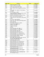
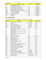
These tables describe the chipset and core POST codes, functions, phases, and components for the POST.
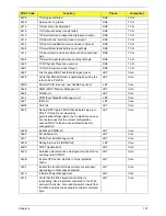
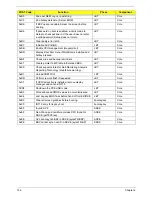
Chipset POST Codes
The following table details the chipset POST codes and functions used in the POST.
POST Code
Function
Phase
Component
0xA0
MRC Entry
PEI
chipset/MRC
0x01
Enable MCHBAR
PEI
chipset/MRC
0x02
Check ME existence
PEI
chipset/MRC
0x03
Check for DRAM initialization interrupt and reset fail
PEI
chipset/MRC
0x04
Determine the system Memory type based on first
populated socket
PEI
chipset/MRC
0x05
Verify all DIMMs are DDR2 and SO-DIMMS, which
are unbuffered
PEI
chipset/MRC
0x06
Verify all DIMMs are Non-ECC
PEI
chipset/MRC
0x07
Verify all DIMMs are single or double sided and not
mixed
PEI
chipset/MRC
0x08
Verify all DIMMs are x8 or x16 width
PEI
chipset/MRC
0x09
Calculate number of Row and Column bits
PEI
chipset/MRC
0x10
Calculate number of banks for each DIMM
PEI
chipset/MRC
0x11
Determine raw card type
PEI
chipset/MRC
0x12
Find a common CAS latency between the DIMMS
and the MCH
PEI
chipset/MRC
0x13
Determine the memory frequency and CAS latency
to program
PEI
chipset/MRC
0x14
Determine the smallest common timing value for all
DIMMS
PEI
chipset/MRC
0x17
Power management resume
PEI
chipset/MRC
0x18
Program DRAM type (DDR2/DDR3) and Power up
sequence
PEI
chipset/MRC
0x19
Program the correct system memory frequency
PEI
chipset/MRC
0x20
Program the correct Graphics memory frequency
PEI
chipset/MRC
0x21
Early DRC initialization
PEI
chipset/MRC
0x22
Program the DRAM Row Attributes and DRAM Row
Boundary registers PRE JEDEC.
PEI
chipset/MRC
0x23
Program the RCOMP SRAM registers
PEI
chipset/MRC
0x24
Program DRAM type (DDR2/DDR3) and Power up
sequence
PEI
chipset/MRC
0x25
Program the DRAM Timing
PEI
chipset/MRC
0x26
Program the DRAM Bank Architecture register
PEI
chipset/MRC
0x27
Enable all clocks on populated rows
PEI
chipset/MRC
0x28
Program MCH ODT
PEI
chipset/MRC
0x29
Program tRD
PEI
chipset/MRC
0x30
Miscellaneous Pre JEDEC steps
PEI
chipset/MRC
0x31
Program clock crossing registers
PEI
chipset/MRC
Содержание Aspire 7230
Страница 6: ...VI ...
Страница 10: ...X Table of Contents ...
Страница 54: ...44 Chapter 2 3 Reboot the system and key in the selected string qjjg9vy 07yqmjd etc for the BIOS user password ...
Страница 85: ...Chapter 3 75 5 Remove the bracket from the board 6 Remove the Finger Print Reader board from the Upper Cover ...
Страница 92: ...82 Chapter 3 4 Grasp the Subwoofer Module and lift it up to remove ...
Страница 94: ...84 Chapter 3 4 Lift the ExpressCard module away from the upper cover ...
Страница 101: ...Chapter 3 91 4 Lift up the bezel and remove it from the LCD Module ...
Страница 105: ...Chapter 3 95 5 Grasp the panel by both ends and lift to remove ...
Страница 107: ...Chapter 3 97 4 Remove the LCD brackets by pulling away from the LCD Panel as shown ...
Страница 110: ...100 Chapter 3 8 Connect the left and right Inverter cables 9 Connect the camera cable ...
Страница 113: ...Chapter 3 103 3 Tighten the four 4 captive screws on the heatsink 4 Connect the Fan cable to the Mainboard ...
Страница 118: ...108 Chapter 3 4 Connect the two FFC cables as shown 5 Connect the cable as shown ...
Страница 206: ...196 Appendix C ...

