


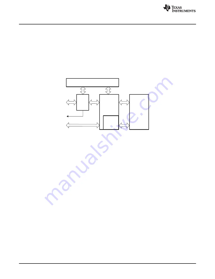
MAB
MDB
Control Registers
MPU
FRAM
Controller
Violation
Cache
FRAM
Memory
Array
FRAM Introduction
5.1
FRAM Introduction
FRAM memory is a nonvolatile memory that reads and writes like standard SRAM. The MSP430 FRAM
memory features include:
•
Byte or word write access
•
Automatic and programmable wait state control with independent wait state settings for access and
cycle times
•
Error correction code with bit error correction capabilities, extended bit error detection and flag
indicators
•
Cache for fast read and endurance improvement
shows the block diagram of the FRAM Controller.
Figure 5-1. FRAM Controller Block Diagram
5.2
FRAM Organization
The FRAM memory can be arranged into segments by the Memory Protection Unit (MPU) (see the
Memory Protection Unit
chapter for details). The address space is linear with the exception of the User
Information Memory and the Device Descriptor Information (TLV).
5.3
FRCTL Module Operation
The FRAM module can be read in a similar fashion to SRAM and has no special requirements. Similarly,
any writes to unprotected segments can be written in the same fashion as SRAM. All writes to user
protected segments are handled as described in the
Memory Protection Unit
chapter.
An FRAM read always requires a write back to the same memory location with the same information read.
This write back is part of the FRAM module itself and requires no user interaction. These write backs are
different from the normal write access from application code.
The FRAM module has built-in error correction code (ECC) logic that is capable of correcting bit errors
and detecting cumulated bit errors. Two flags are available to indicate the presence of an error. The
CBDIFG is set when a correctable bit error has been detected and corrected. If CBDIE is also set, a
System NMI event (SYSNMI) occurs. The UBDIFG is set when a cumulated bit error that is not
correctable has been detected. If UBDIE is also set, a System NMI event (SYSNMI) occurs. Upon
correctable or uncorrectable bit errors, the program vectors to the SYSSNIV if the NMI is enabled. If
desired, a System Reset event (SYSRST) can be generated by setting the UBDRSTEN bit. If an
uncorrectable error is detected, a PUC is initiated and the program vectors to the SYSRSTIV.
244
FRAM Controller (FRCTL)
SLAU272C – May 2011 – Revised November 2013
Copyright © 2011–2013, Texas Instruments Incorporated